IKEA Koppla USB Supply Clears Teardown With Robust Mains Isolation
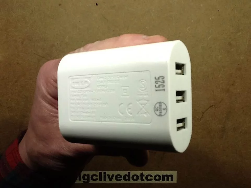
bigclivedotcom
A teardown reveals the budget adapter incorporates multi-layer transformer shielding, inrush protection, and a molded plastic isolation blade that eliminate shock hazards common in low-cost chargers.
AI-assisted summary of Teardown of an IKEA Koppla USB power supply. — original source. Check the original for full context.
Source published:
Key ideas
- Destructive teardown of the IKEA Koppla 3.4A USB power supply confirms it adheres to rigorous safety standards, contrasting sharply with dangerous fakes that can have as little as 2 mm of isolation between mains and low-voltage rails. (0:00)
- Leakage current on the double-insulated IKEA Koppla measured at 64 µA, well below the ~100 µA observed on an unearthed genuine Apple charger. (2:30)
- Internal dissection reveals complex safety engineering, including an interleaved split-primary transformer, a grounded trifilar electrostatic screen, and double-insulated secondary wire. (12:48)
- The enclosure and PCB feature robust physical isolation, combining a routed board slot with an integrated molded plastic barrier blade and spark gaps rated to ~10 kV. (10:27)
Detailed notes
## Background Published on YouTube by bigclivedotcom on April 8, 2016, this teardown video examines an IKEA Koppla multi-port USB power supply. Big Clive takes the unit apart to evaluate its electrical safety, galvanic isolation, and internal transformer construction in line with his general recommendation to use prominent brand chargers.
## TL;DR Big Clive disassembles an IKEA Koppla 3-port USB power supply to evaluate its build quality and safety compared to dangerous counterfeit chargers. After measuring a compliant 64 µA leakage current and cracking the welded case, he inspects the PCB's robust input protection, inrush thermistor, common-mode filtering, and auto-detect charging ICs. He then completely unwinds the high-frequency transformer, uncovering a well-designed interleaved sandwich construction with electrostatic Faraday shielding and thick secondary wire insulation. Finding strong thermal planning, milled PCB isolation slots, and an internal plastic barrier blade, Clive concludes the charger is exceptionally well-engineered and safe to recommend.
## Atmosphere & style The presentation is calm, methodical, and delightfully geeky, driven by Clive's characteristic Scottish lilt, gentle dry humor, and hands-on bench curiosity. While destructive teardowns of functioning equipment carry a lighthearted sense of 'criminal' guilt, the video treats safety hazards with genuine gravity, contrasting the Koppla's solid construction against terrifying cheap clones. Watching it feels like looking over the shoulder of an expert tinkerer patiently peeling back layers of magnet wire and lacquer to reveal the hidden craftsmanship inside an ordinary household object.
## Bulletin - [00:00](https://www.youtube.com/watch?v=uRe9w5PKmsE&t=0s) Destructive teardown of the IKEA Koppla 3.4A USB power supply confirms it adheres to rigorous safety standards, contrasting sharply with dangerous fakes that can have as little as 2 mm of isolation between mains and low-voltage rails. - [02:30](https://www.youtube.com/watch?v=uRe9w5PKmsE&t=150s) Leakage current on the double-insulated IKEA Koppla measured at 64 µA, well below the ~100 µA observed on an unearthed genuine Apple charger. - [12:48](https://www.youtube.com/watch?v=uRe9w5PKmsE&t=768s) Internal dissection reveals complex safety engineering, including an interleaved split-primary transformer, a grounded trifilar electrostatic screen, and double-insulated secondary wire. - [10:27](https://www.youtube.com/watch?v=uRe9w5PKmsE&t=627s) The enclosure and PCB feature robust physical isolation, combining a routed board slot with an integrated molded plastic barrier blade and spark gaps rated to ~10 kV.
## Key takeaways - [00:00](https://www.youtube.com/watch?v=uRe9w5PKmsE&t=0s) Counterfeit and bargain chargers present severe hazards, frequently lacking galvanic isolation or routing live mains tracks within millimeters of low-voltage DC rails. - [02:30](https://www.youtube.com/watch?v=uRe9w5PKmsE&t=150s) Genuine Apple chargers can exhibit around 100 µA of leakage current due to heavy RF suppression filtering when used with ungrounded UK plug adapters. - [02:30](https://www.youtube.com/watch?v=uRe9w5PKmsE&t=150s) The IKEA Koppla delivers a stable 3.4A overall output without voltage droop and maintains a safe leakage current of 64 µA as a Class II double-insulated unit. - [04:15](https://www.youtube.com/watch?v=uRe9w5PKmsE&t=255s) The primary stage incorporates robust protection, including an NTC inrush current limiter, common-mode choke, and a Pi-filter smoothing network. - [08:08](https://www.youtube.com/watch?v=uRe9w5PKmsE&t=488s) Each USB port integrates an autonomous auto-detect SOT-23 chip on the D+/D- lines to negotiate charging profiles up to 2.1A per port. - [08:08](https://www.youtube.com/watch?v=uRe9w5PKmsE&t=488s) Thermal management separates heat-sensitive electrolytic capacitors from the diode heatsink, utilizing natural convection inside the enclosure. - [10:27](https://www.youtube.com/watch?v=uRe9w5PKmsE&t=627s) PCB spark gaps rated for approximately 10 kV protect internal components against severe electrostatic discharge introduced through the USB ports. - [10:27](https://www.youtube.com/watch?v=uRe9w5PKmsE&t=627s) The high-frequency transformer features asymmetric keyed pins to eliminate reverse-insertion assembly errors. - [11:45](https://www.youtube.com/watch?v=uRe9w5PKmsE&t=705s) The primary switch-mode IC relies on a combined bootstrap and auxiliary feedback winding to sustain continuous power and monitor output voltage. - [12:48](https://www.youtube.com/watch?v=uRe9w5PKmsE&t=768s) The ferrite core is physically shielded by a tinned copper wire bonded directly to the primary negative rail to mitigate electromagnetic interference. - [17:19](https://www.youtube.com/watch?v=uRe9w5PKmsE&t=1039s) Electrostatic screening between the primary and secondary is achieved via an insulated, grounded trifilar copper winding rather than traditional copper foil. - [20:26](https://www.youtube.com/watch?v=uRe9w5PKmsE&t=1226s) A split-primary sandwich winding topology minimizes leakage inductance while fully protecting the triple-insulated secondary wire. - [27:07](https://www.youtube.com/watch?v=uRe9w5PKmsE&t=1627s) A physical plastic blade molded into the case protrudes through the routed PCB isolation slot to guarantee creepage barrier separation. - [27:07](https://www.youtube.com/watch?v=uRe9w5PKmsE&t=1627s) Clive strongly endorses the IKEA Koppla, concluding that its bespoke design and redundant safety features make it an exceptionally well-engineered budget charger.
## Detailed walkthrough ### [00:00](https://www.youtube.com/watch?v=uRe9w5PKmsE&t=0s) USB Power Supply Safety and Dangerous Fakes
Clive begins by explaining his general philosophy on buying USB chargers. For a long time, he has advised viewers to stick to major, reputable brands. He frequently recommends genuine Apple chargers—clarifying that this is not out of brand loyalty, but because Apple is a massive corporation with a strong interest in protecting its reputation, leading them to design well-engineered, high-standard power supplies. He points out how critical 5V USB supplies have become in everyday life, powering everything from smartphones to desk lamps. However, this ubiquity brings severe safety hazards when consumers end up with counterfeit or poorly designed hardware.
Reflecting on past teardowns—such as a hazardous unit that had 240 volts live on exposed surfaces—Clive highlights how dangerous cheap chargers can be. He presents an imitation Apple charger that appears convincing on the surface, but teardowns reveal a terrifying design flaw: just 2 millimeters of physical isolation separating the high-voltage mains from the low-voltage DC rails. He shows a counterfeit charger branded as "Samsung," noting that genuine Samsung units would never be built like this. The fake simply routes low-voltage and mains tracks right next to each other at standard spacing across the board, completely lacking safety isolation.
He also showcases a budget charger purchased from Flying Tiger Copenhagen ("Tiger"), a retail chain with global stores known for novelty goods. Having previously torn down a purple variant, Clive considers Tiger units surprisingly decent—definitely a cut above no-name knockoffs—though, at around £5 including a cable, they cannot be expected to match the high engineering standards of premium brands.
> “So, it makes sense to get yourself a beefy, chunky, good quality supply that's safe.” — Clive
- **Counterfeit Apple Charger**: Features only 2 mm of clearance between mains and the low-voltage side, making it an extreme hazard. - **Counterfeit Samsung Charger**: Lacks galvanic isolation; high-voltage AC and low-voltage DC copper tracks run side-by-side without dedicated clearance. - **Tiger (Flying Tiger) Charger**: Sells for roughly £5 with a cable; far superior to generic fakes, but still built to budget constraints.
---
[02:30](https://www.youtube.com/watch?v=uRe9w5PKmsE&t=150s) Comparing Apple and IKEA: Grounding and Leakage Current
Clive turns his attention to the genuine Apple charger and its design eccentricities. The Apple unit is modular, built with swappable plug adapters for international travel. It features a round metal stud on the back meant for sliding on country-specific mains pins. Interestingly, this metal pin connects internally toward the chassis and the negative rail to establish an earth reference. However, the UK three-pin plug adapter supplied with it does not include an internal mating contact for that stud, leaving the unit effectively unearthed in practice. Because of Apple's extensive, aggressive RF suppression filtering, Clive measured a leakage current of around 100 microamps (µA) on the Apple unit, meaning it is noticeably prone to giving users a mild electric tingle when brushed against.
In comparison, Clive measured the IKEA Koppla charger's leakage current at 64 µA, which is typical and well within expected norms for a double-insulated power supply. He observes that IKEA's packaging and manual include roughly 35 languages to accommodate international distribution. Because many global markets do not have earthed wall outlets, IKEA designs the Koppla as a Class II, double-insulated supply rather than relying on an earth pin. Clive notes that while a user might occasionally perceive a faint tingle on the sensitive skin of their hands due to the capacitive leakage inherent to switch-mode power supplies, the unit is stable. The IKEA Koppla is rated for an overall output of 3.4 amps; Clive tested it up to a 2 amp load and confirmed that it maintained its output voltage without drooping.
> “And you are likely if in some scenarios you'll get a very faint tingle, particularly in the back of your hand if you brush against something while you're holding an object that's plugged into this.” — Clive
- **Apple Charger Leakage**: Measured at ~100 µA due to substantial RF suppression capacitor filtering. - **IKEA Koppla Leakage**: Measured at 64 µA, comfortably compliant with double-insulated standards. - **IKEA Koppla Total Rating**: 3.4 A across its USB ports; verified stable under Clive's 2 A benchmark test.
---
[04:15](https://www.youtube.com/watch?v=uRe9w5PKmsE&t=255s) Cracking the Koppla Case and Primary Filtering Stage
Opening the IKEA Koppla proves to be a physical challenge. Knowing that IKEA products are tightly snapped together or ultrasonically welded, Clive pauses the recording to avoid forcing the audience to endure the wrestling match. He returns after cracking the enclosure using a hammer and a pair of pipe grips. Inside, the shell incorporates plastic alignment pins, though the strength of the seal suggests it was glued or welded rather than just clipped. To inspect the circuit board freely, he snips the primary input leads.
```mermaid flowchart LR accTitle: Koppla Primary Input Stage Flowchart accDescr: Flow diagram showing mains AC input passing through NTC thermistor, common mode choke, bridge rectifier, and Pi-filter.
subgraph Primary_Protection["Mains Input & Inrush"] AC["Mains Input"] --> NTC["NTC Thermistor<br/>(NTC1)"] end
subgraph Filtration["EMI & Rectification"] NTC --> CMC["Common Mode<br/>Choke"] CMC --> BR["Surface-Mount<br/>Bridge Rectifier"] end
subgraph Smoothing["DC Smoothing"] BR --> C1["Smoothing<br/>Capacitor 1"] C1 --> L1["Inductor<br/>Choke"] L1 --> C2["Smoothing<br/>Capacitor 2"] C2 --> PWM["Switch-Mode<br/>Controller & FET"] end ```
Examining the printed circuit board, Clive immediately praises the professional layout, highlighting clean track isolation and integrated spark gaps on the high-voltage side. The mains input passes directly through an NTC (negative temperature coefficient) thermistor labeled `NTC1`. The NTC acts as an inrush current limiter; when cold, its higher initial resistance suppresses current spikes that occur when charging empty primary filter capacitors, preventing household breakers or power strips from tripping on plug-in. Following the NTC, the line passes through a common-mode choke—where live and neutral are wound in opposing directions on a single core so that 50 Hz AC passes unhindered while high-frequency noise and switching transients induce opposing magnetic fields that cancel out. The AC is rectified by a dedicated surface-mount bridge rectifier with well-spaced corner solder pads, followed by a pi-filter arrangement consisting of a first smoothing capacitor, an inductor choke, and a second smoothing capacitor to thoroughly eliminate ripple before reaching the primary switching transistor and controller IC.
> “Oh, look at the severation. Uh oh, look at the spark gaps and everything. This is this is like pro.” — Clive
- **Enclosure Fastening**: Sealed securely using heavy internal plastic alignment pins and adhesive/welding, requiring pipe grips and a hammer to crack open. - **Inrush Protection**: Negative Temperature Coefficient thermistor (`NTC1`) prevents primary capacitor surge currents from tripping breakers. - **EMI Suppression**: Common-mode inductor choke blocks high-frequency differential/transient noise from leaking back into the mains grid. - **Mains Rectification & Smoothing**: Surface-mount bridge rectifier arranged with corner pads for maximum separation, followed by a dual-capacitor and choke Pi-filter network.
---
[08:08](https://www.youtube.com/watch?v=uRe9w5PKmsE&t=488s) Primary Switcher, Secondary Rectifier, and Port Controllers
Looking closely at the active electronics, Clive identifies the primary switch-mode power supply controller, noting obscure markings that read roughly `1699-02 R5 1 gh`. It drives an external switching transistor, which feeds the high-frequency transformer. Clive remarks that while destructive teardowns of functional, high-quality hardware feel almost criminal, destructive testing is necessary because external appearances can be deceiving—as seen on previous teardowns where neat transformers concealed dangerous internal wiring.
On the secondary side, rectified 5V DC is produced via a heavy diode mounted to its own dedicated heatsink. Clive approves of the component layout, noting that the sensitive electrolytic smoothing capacitors on the output have been intentionally positioned away from the diode’s heatsink to protect them from heat degradation. Looking closely at each USB output port, he spots tiny SOT-23-style surface-mount ICs bearing miniature laser-etched markings reading `1988 D` and `GIC CER`. He explains that each port has one of these dedicated auto-detect chips connected across the 5V and 0V power rails with outputs routed to the USB $D+$ and $D-$ data pins. These chips actively negotiate charging profiles with connected devices (such as phones and tablets), signaling to the connected gadget that the port can deliver up to its individual rating of 2.1 amps.
> “It feels a criminal thing taking this power supply, you know, to bits and ruining it when it's a perfectly good working power supply. But if I do it, uh, you guys don't have to.” — Clive
- **Primary PWM Controller Markings**: Marked with `1699-02 R5 1 gh`, driving a separate power switching transistor. - **Output Diode**: Mounted directly to a metal heatsink; Clive highlights that output filter capacitors are spaced away from this heat source to prevent premature drying out. - **Per-Port USB Auto-Detect ICs**: Tiny SOT-23 packaged chips marked `1988 D` bridge the power rails to the data pins ($D+/D-$) to communicate with connected devices and authorize up to 2.1 A charging rates.
[10:27](https://www.youtube.com/watch?v=uRe9w5PKmsE&t=627s) Isolation Gaps, Spark Gaps, and Transformer Removal
Big Clive inspects the isolation boundary on the circuit board, noting an exceptionally wide physical gap that features an actual routed cutout across the substrate alongside the Class-Y safety capacitor. He also spots two integrated PCB spark gaps across the isolation barrier. He deduces these serve as a protective fail-safe against electrostatic discharge (ESD) introduced via the output ports:
> “You know, if you go to plug something and you've got a high static charge, it means that if the voltage exceeds the rating of all these components as a last resort, it can jump physically across as a spark.”
He estimates that crossing this gap would require roughly 10 kV. Turning his attention to the Class-Y suppression capacitor, he checks the marking to verify whether it is 10 nF before confirming it is actually a 1 nF capacitor.
To inspect the transformer's internal build quality, Clive desolders it from the board. Because the Koppla uses a single-sided printed circuit board, the transformer comes out cleanly without fighting through-plated holes. Examining the removed component, Clive appreciates the deliberate pin design: the pins on one side are aligned sideways, while the opposite side is aligned longways. This asymmetry guarantees proper orientation during assembly and prevents accidental reverse insertion.
- **Isolation Routing:** PCB slot cut out beneath the Class-Y capacitor to extend creepage distance. - **Spark Gap Threshold:** Estimated ~10 kV breakdown voltage to protect primary components from ESD. - **Class-Y Capacitor Value:** 1 nF. - **Transformer Pinout:** Asymmetric pin alignment (transverse vs. longitudinal) for foolproof keyed mounting.
---
[11:45](https://www.youtube.com/watch?v=uRe9w5PKmsE&t=705s) Switch-Mode Architecture and Bootstrap Circuits
Clive examines the pinout and circuit topology of the transformer. It follows the standard architecture for modern switch-mode power supplies, containing a high-voltage primary winding, an auxiliary winding on the mains side, and an isolated low-voltage secondary output feeding the 5V rail. Clive explains that the auxiliary winding is not solely a bootstrap winding; it functions as combined bootstrap and voltage feedback.
When the power supply is initially plugged into the mains, there is a brief startup delay while a tiny capacitor charges through a high-value dropper resistor. Once that capacitor reaches operating threshold, the controller chip switches on and starts pulsing the transformer. At that point, the auxiliary winding generates power through a rectifier diode to run the IC continuously—effectively sustaining its own power supply while simultaneously monitoring output voltage behavior via magnetic coupling. Clive remarks on how component-dense the board is compared to typical budget switch-mode adapters:
> “In fact this is for a a modern switch power supply. This is a lot of support components. It's really quite a complex uh unit.”
The third winding provides the galvanic isolation separating the lethal 300 V DC bus from the 5V USB output that users come into direct contact with.
```mermaid flowchart TD accTitle: Koppla Primary Bootstrap and Auxiliary Supply Loop accDescr: Diagram illustrating how the primary IC starts via a high-value resistor and self-powers via the auxiliary winding. subgraph Startup ["Mains Startup Phase"] Mains["~300V DC Rail"] -->|"High-value resistor"| Cap["Small Startup Capacitor"] Cap -->|"Threshold reached"| IC["Control IC Starts Switching"] end subgraph Running ["Running Phase"] IC -->|"Drives switching pulse"| Pri["Transformer Primary"] Pri -->|"Inductive coupling"| Aux["Auxiliary / Feedback Winding"] Aux -->|"Diode rectified"| IC Pri -->|"Galvanic isolation"| Sec["5V Secondary (User Touch Safe)"] end ```
---
[12:48](https://www.youtube.com/watch?v=uRe9w5PKmsE&t=768s) Dissecting the Transformer: Shielding and the Outer Primary
Clive begins dismantling the transformer by slicing through the outer insulating tape. He observes that all flying leads on the mains side have protective sleeving applied where they exit the coil, and the transformer casing features an ink-stamped part number and date code. However, tearing into the core proves difficult: the ferrite core is housed inside a dedicated plastic shell and heavily potted in hard lacquer.
After applying force with a screwdriver to crack open the glued assembly, Clive uncovers a peculiar construction detail: a bare copper wire, tinned at its contact point and tied directly to the primary negative rail, is wrapped tightly around the outside of the bare ferrite core and glued in place with lacquer. He identifies this as an uncommon measure to ground and screen the ferrite core against electromagnetic interference.
Peeling back the outer layer of polyester tape, Clive starts unwinding the first copper layer. Expecting an auxiliary feedback winding, he traces the connection and realizes it is actually an interleaved outer section of the primary winding tied directly to the positive rail:
> “And the secondary does have that thick insulation which is intact which is good. That was the weakness. That was the failing point in the squeeze unit. the secondary in insulation had been violated.”
This outer primary layer runs cleanly across the bobbin without encroaching on the secondary side, terminating at a center-tap loop that passes beneath the tape to join the deeper primary winding.
---
[17:19](https://www.youtube.com/watch?v=uRe9w5PKmsE&t=1039s) The Mysterious Multi-Strand Screening Layer
Underneath the outermost primary section, Clive uncovers what initially appears to be an anomalous loose connection: a small cluster of wires folded into the bobbin that appears to terminate nowhere. For a moment, he wonders if he snapped a lead or stumbled across an open, single-ended capacitive feedback pickup.
Unwinding the layer reveals a ribbon of three parallel copper strands wrapped around the circumference of the coil. All three strands join together at one end to a single pin on the primary side, while their opposing ends are clipped flush and insulated under the tape barrier. Clive recognizes this as a multi-wire electrostatic Faraday shield, designed to block high-frequency common-mode noise between the primary and secondary windings:
> “Sometimes I think there's a you know the switch mode power supplies is a bit of a black art at times that the high frequencies that operate at just normal rules do not apply.”
Rather than using a solid strip of copper tape with an insulating gap—as was done in the dangerous generic "Squeeze" power supply he previously reviewed—this transformer achieves electrostatic shielding using a parallel trifilar wire winding grounded at a single node.
---
[20:26](https://www.youtube.com/watch?v=uRe9w5PKmsE&t=1226s) The Secondary and Inner Primary Layers
Continuing inward, Clive reaches the secondary winding. Where the secondary leads cross adjacent primary and feedback connections, the crossing wires are protected with auxiliary sleeves. The secondary itself is wound from thick, double-insulated wire (reinforced three-layer or triple-insulated winding wire). Unlike cheap counterfeit chargers where tight winding machines scrape away fragile enamel insulation, this heavy insulation remains fully intact across the entire run.
Beneath another tight barrier of polyester tape lies the auxiliary feedback winding. Clive unravels this layer and finds it is wound with a parallel cluster of three wire cores that connect to the middle pin feeding the IC via a diode, with the return line tied to the primary ground.
Finally, Clive reaches the bottom of the bobbin and unwinds the inner primary winding. This section consists of a dense count of enameled wire turns running directly onto the center plastic bobbin spindle, completing the connection to the primary switching transistor loop. Clive confirms that the transformer utilizes a classic split-primary sandwich structure (interleaving the secondary and auxiliary between an inner and outer primary layer) to minimize leakage inductance while maintaining robust dielectric isolation:
> “So, so far it does look like it's a been a sensibly designed transformer and care has been made, you know, taken in making it. So, um, coupled with the other features here, the isolation features, this does look, as you'd expect from IKEA, it does look quite a well-designed supply.”
| Layer (Outside to Inside) | Type / Conductor | Electrical Termination & Safety Details | |:--- |:--- |:--- | | **External Core Wrap** | Tinned bare copper wire | Glued to ferrite core; bonded to primary negative rail for EMI shielding. | | **Layer 1 (Outer Primary)** | Magnet wire with end sleeving | Connects to positive rail; forms the outer half of the split primary. | | **Layer 2 (Faraday Screen)** | 3-wire cluster (trifilar) | Connected to a single primary pin at one end; free end left floating. | | **Layer 3 (Secondary)** | Heavy double-insulated wire | Feeds 5V output; sleeves protect intersections with other pins. | | **Layer 4 (Aux / Feedback)** | 3-wire cluster (trifilar) | Drives IC supply rail via rectifier diode; tied to primary negative. | | **Layer 5 (Inner Primary)** | High-turn count magnet wire | Wound directly onto the central plastic bobbin; handles ~300 V switching. |
[25:41](https://www.youtube.com/watch?v=uRe9w5PKmsE&t=1541s) Internal Layout, Thermal Design, and Wiring Quality
Examining the exposed board and transformer, Big Clive remarks on how surprisingly complex the unit is, noting the sheer volume of supporting components surrounding the unusual transformer. Despite the complexity, everything in the construction checks out as well-designed. The circuit features robust input filtering, inrush current limiting, and modest, supported heatsinks on both the primary switching side and secondary rectifier diode side rather than components flapping loose on their leads. Between the high-voltage mains and low-voltage secondary circuitry, the board features generous creepage distances, spark gaps, and an isolation slot milled right through the PCB where the transformer windings cross over. Furthermore, the electrolytic capacitors are deliberately kept away from the heatsinks to avoid heat-induced degradation.
Clive observes that the physical orientation of the charger when plugged into a wall outlet works to its thermal advantage. As installed, heat rising off the heatsinks naturally drifts toward the top of the casing, carrying thermal energy away from the sensitive capacitors below. Small ventilation openings visible in the USB port frames allow for a modest amount of air circulation, at least until all three ports are plugged in under maximum load. He also praises the primary mains connections coming off the rear prongs, which use heavy, high-rated wire with two layers of insulation rather than the flimsy, hair-thin wires commonly encountered in cheap generic imports.
- Built with dedicated inrush current limiting and comprehensive mains filtering. - Rigidly mounted, supported heatsinks for both the primary transistor and the secondary rectifier diode. - Physical isolation slot milled through the PCB beneath the transformer to separate mains potential from low-voltage rails. - Heavy-gauge mains lead-in wires featuring dual-layer insulation.
---
[27:07](https://www.youtube.com/watch?v=uRe9w5PKmsE&t=1627s) Enclosure Construction, Isolation Blade, and Final Verdict
Turning his attention back to the plastic casing, Clive removes two screws near the mains pin assembly to see if the plug section detaches as part of a modular universal casing for different regional adapters. Although the outer cover is clipped tightly in place and does not easily separate, he notes that it appears to be an assembly tailored specifically for the UK variant. Surveying the disassembled parts spread across his bench, he jokingly acknowledges that the disassembled charger is a “wondrous mess that's never ever going to go back together again,” but remains impressed with its build quality.
```mermaid flowchart TD accTitle: Koppla Physical Safety and Retention Layout accDescr: Diagram illustrating how the enclosure case interacts with the PCB via plastic blades and anchor pillars.
subgraph Enclosure["Molded Outer Casing"] Blade["Molded Plastic Isolation Blade"] Pillars["3x Internal Anchoring Pillars"] end
subgraph PCB["Power Supply Circuit Board"] Slot["Milled Isolation Slot"] MountPoints["Firm Retention Points"] end
Blade -->|"Protrudes through"| Slot Pillars -->|"Firmly clamp into place"| MountPoints ```
He highlights two final engineering details molded directly into the housing. First, the isolation gap cut through the circuit board aligns directly with an internal molded plastic blade on the case shell; when assembled, this plastic fin slides completely through the slot to create a physical barrier between the primary and secondary domains. Second, the case incorporates three rigid anchoring posts—one at the top and two near the base—that clamp down on the board to keep it locked firmly in position. Impressed by the safety engineering, Clive gives the unit an emphatic endorsement: “Would I buy another IKEA power supply like this? I think I would. It seems to be quite well engineered.”
- Internal plastic blade protrudes entirely through the milled circuit board slot to enforce physical barrier isolation between mains and low-voltage rails. - Three molded internal retention posts clamp the PCB securely in place against physical shock. - Overall construction indicates a product thoroughly designed from scratch with deliberate attention to electrical safety standards.
## Notable quotes > [00:00](https://www.youtube.com/watch?v=uRe9w5PKmsE&t=0s) So, it makes sense to get yourself a beefy, chunky, good quality supply that's safe. — Clive
> [27:07](https://www.youtube.com/watch?v=uRe9w5PKmsE&t=1627s) Would I buy another IKEA power supply like this? I think I would. It seems to be quite well engineered. — Clive
## Mentioned IKEA, IKEA Koppla, Apple, Samsung, Flying Tiger Copenhagen, bigclivedotcom
## Video description I've always recommended using prominent brand USB chargers for safety. So I thought I'd take an IKEA one to bits and assess it for safety with regards to isolation and transformer construction.
If you enjoy the videos on this channel you can help support it with a dollar for coffee, cookies and things to take apart at https://www.patreon.com/bigclive
[Source](https://www.youtube.com/watch?v=uRe9w5PKmsE)