Ben Eater Decodes PS/2 Keyboard Signals Using Cascaded Shift Registers
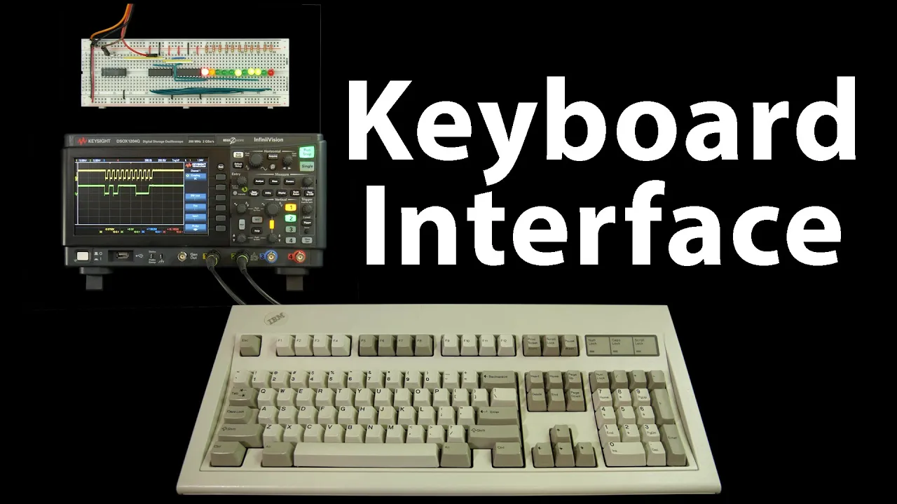
So how does a PS/2 keyboard interface work? — Ben Eater

Ben Eater

Because PS/2 keyboards emit raw multi-byte make-and-break scancodes without native ASCII mapping, host systems must rely on hardware buffers, interrupts, or preprocessors to reconstruct keystroke state.

AI-assisted summary of So how does a PS/2 keyboard interface work? — original source. Check the original for full context.

Source published:

Key ideas

  • The standard PS/2 keyboard interface operates over four active lines—power, ground, clock, and serial data—transmitting 11-bit frames per event clocked on falling edges. (0:00)
  • Converting serial PS/2 bitstreams to parallel data using 74HC595 shift registers requires inverting the keyboard clock and inserting an inverter delay stage to prevent latching hazards. (4:38)
  • Key events are communicated via arbitrary scancodes, break prefixes (F0), and extended prefixes (E0), requiring the host system to manage key state, modifiers, and multi-byte framing. (23:41)
  • PS/2 host interfaces can be implemented through cascaded shift register hardware buffers, direct interrupt service routines, or intermediate microcontrollers that translate scancodes directly to ASCII. (30:25)

Detailed notes

## Background This video was published on YouTube by Ben Eater on March 6, 2021. According to the page description, it explores how a PS/2 keyboard interface works, providing a link to a list of scancodes and pointing viewers to eater.net for computer engineering resources and 6502 computer kits.

## TL;DR Ben Eater reverse-engineers the signaling and protocol of a standard PS/2 keyboard to interface it with breadboard hardware. By probing the physical pinout and inspecting clock and data lines on an oscilloscope, he demonstrates that keystrokes transmit as 11-bit serial frames comprising start, data, parity, and stop bits. Using 74HC04 inverters to correct clock polarity and propagation delay, he cascades 74HC595 shift registers to capture, latch, and visually display the serial stream on LEDs. Through this hardware, he decodes raw scancodes, explains make and break codes, analyzes multi-byte sequences for extended keys, and discusses system-level interface architectures for host microprocessors like the 6502.

## Atmosphere & style The presentation carries Ben Eater's signature calm, methodical, and deeply instructional rhythm. It feels like leaning over a quiet electronics workbench alongside an experienced engineer who inspects every wire, waveform, and logic level with deliberate clarity. The tone is practical, patient, and inquisitive, shifting naturally from basic continuity testing to deep protocol exploration with quiet satisfaction as rows of breadboard LEDs progressively untangle the keyboard's serial stream.

## Bulletin - [00:00](https://www.youtube.com/watch?v=7aXbh9VUB3U&t=0s) The standard PS/2 keyboard interface operates over four active lines—power, ground, clock, and serial data—transmitting 11-bit frames per event clocked on falling edges. - [04:38](https://www.youtube.com/watch?v=7aXbh9VUB3U&t=278s) Converting serial PS/2 bitstreams to parallel data using 74HC595 shift registers requires inverting the keyboard clock and inserting an inverter delay stage to prevent latching hazards. - [23:41](https://www.youtube.com/watch?v=7aXbh9VUB3U&t=1421s) Key events are communicated via arbitrary scancodes, break prefixes (F0), and extended prefixes (E0), requiring the host system to manage key state, modifiers, and multi-byte framing. - [30:25](https://www.youtube.com/watch?v=7aXbh9VUB3U&t=1825s) PS/2 host interfaces can be implemented through cascaded shift register hardware buffers, direct interrupt service routines, or intermediate microcontrollers that translate scancodes directly to ASCII.

## Key takeaways - [00:00](https://www.youtube.com/watch?v=7aXbh9VUB3U&t=0s) A standard PS/2 6-pin mini-DIN interface requires only four physical lines: +5V power, ground, synchronous clock, and serial data. - [03:25](https://www.youtube.com/watch?v=7aXbh9VUB3U&t=205s) Oscilloscope inspection reveals that the keyboard outputs synchronous serial data bits aligned with dedicated clock pulses. - [04:38](https://www.youtube.com/watch?v=7aXbh9VUB3U&t=278s) The PS/2 clock rests high and transmits data valid on its falling edge, necessitating an inverter to trigger rising-edge 74HC595 shift register clocks. - [09:50](https://www.youtube.com/watch?v=7aXbh9VUB3U&t=590s) Connecting the shift clock directly to the latch clock introduces a race condition that can be resolved by passing the signal through two spare inverter gates for propagation delay. - [19:21](https://www.youtube.com/watch?v=7aXbh9VUB3U&t=1161s) Every PS/2 transmission consists of an 11-bit frame: a 0 start bit, eight data bits, an odd parity bit, and a 1 stop bit. - [13:10](https://www.youtube.com/watch?v=7aXbh9VUB3U&t=790s) Cascading multiple 74HC595 shift registers by chaining serial out to serial in enables the capture of packets exceeding 8 bits. - [17:07](https://www.youtube.com/watch?v=7aXbh9VUB3U&t=1027s) PS/2 keyboards do not transmit ASCII characters; instead, they output arbitrary scan codes (e.g., 2E for '5', 16 for '1') that require external decoding. - [23:41](https://www.youtube.com/watch?v=7aXbh9VUB3U&t=1421s) Standard key releases trigger an explicit break code composed of prefix F0 followed by the key's original make code. - [21:15](https://www.youtube.com/watch?v=7aXbh9VUB3U&t=1275s) Extended keys, such as navigation keys, emit the E0 prefix during press and produce three-byte sequences (E0 F0 [scancode]) upon release. - [26:52](https://www.youtube.com/watch?v=7aXbh9VUB3U&t=1612s) The keyboard hardware has no internal concept of capitalization; typing capital 'A' produces separate make and break events for Shift and A that the host must track. - [28:47](https://www.youtube.com/watch?v=7aXbh9VUB3U&t=1727s) Many extended navigation keys share base scancodes with the numeric keypad (e.g., Home and Keypad 7 sharing 6C) due to historical PC keyboard evolution. - [28:47](https://www.youtube.com/watch?v=7aXbh9VUB3U&t=1727s) Special keys exhibit extreme protocol outliers, such as Pause sending an eight-byte sequence with no break code, and Print Screen requiring multi-byte make and break bursts. - [28:47](https://www.youtube.com/watch?v=7aXbh9VUB3U&t=1727s) Keyboard status LEDs (like Num Lock) are not toggled locally by the keyboard, but require bidirectional control commands from the host computer. - [30:25](https://www.youtube.com/watch?v=7aXbh9VUB3U&t=1825s) Interfacing a PS/2 keyboard to a microprocessor can be achieved via memory-mapped shift register buffers, CPU interrupt routines, or dedicated microcontroller preprocessors.

## Detailed walkthrough ### [00:00](https://www.youtube.com/watch?v=7aXbh9VUB3U&t=0s) Identifying the PS/2 Connector Pinout

Keyboards remain among the most familiar input devices in computing, and for decades the PS/2 interface was ubiquitous across personal computers. Because of its conceptual and electrical simplicity, it serves as an ideal peripheral interface for breadboard projects, such as a custom home-built 6502 computer. Ben Eater points out that anyone interested in constructing one can find kits and design videos at eater.net/6502.

A standard PS/2 port features a 6-pin mini-DIN connector, but only four pins are actively utilized: two supply electrical power, while the remaining two carry the clock and data signals that convey keystroke information. To interface with the keyboard, Ben takes an extension cable with a mating female PS/2 receptacle, snips the opposite end off, and strips away the outer jacket. Inside the shielding lie four thin conductors: red, black, orange, and brown. Ben strips these delicate wires using his fingernails and twists the wire strands together to prepare them for testing.

```mermaid flowchart TD accTitle: PS/2 Mini-DIN Pinout Mapping accDescr: Mapping of the four active pins of a PS/2 mini-DIN connector to wire colors and roles.

subgraph Connector["PS/2 6-Pin Mini-DIN"] P3["Pin 3: Ground"] P4["Pin 4: +5V Power"] P1["Pin 1: Data"] P5["Pin 5: Clock"] end

subgraph Harness["Stripped Cable Wires"] W_Orange["Orange Wire (+ Shield)"] W_Black["Black Wire"] W_Red["Red Wire"] W_Brown["Brown Wire"] end

P3 --> W_Orange P4 --> W_Black P1 --> W_Red P5 --> W_Brown ```

Using a digital multimeter in continuity mode, Ben probes between the physical socket pins and the bare wires to determine the harness pinout. The pinout reveals a somewhat counterintuitive color scheme:

- **Pin 3 (Ground):** Connects to the orange wire; Ben twists this lead together with the cable's braided shield ground. - **Pin 4 (+5V VCC):** Traces to the black wire, prompting Ben to remark on the confusing choice: “So 5 volts is black that figures it's kind of confusing.” - **Pin 1 (Data):** Traces to the red wire. - **Pin 5 (Clock):** Traces to the brown wire.

Connecting a standalone 5V DC power adapter, Ben wires +5V to the black wire and ground to the orange wire and shield braid using jumper leads. Leaving clock and data unconnected, he plugs the keyboard into the cable socket. The keyboard status indicator LEDs flash momentarily on power-up, verifying that the keyboard is receiving power.

---

[03:25](https://www.youtube.com/watch?v=7aXbh9VUB3U&t=205s) Probing Clock and Data Signals on the Oscilloscope

To observe the keystroke signaling directly, Ben attaches two oscilloscope probes to the harness: the primary ground clip clamps to the keyboard ground wire, channel one connects to the clock lead (brown), and channel two taps the serial data line (red).

Upon pressing and releasing keys on the keyboard, bursts of activity appear across both oscilloscope channels. Zooming in on the waveforms reveals a synchronous serial transmission: the clock line outputs a distinct train of discrete pulses, while the data trace transitions between logic high (+5V) and logic low (0V). On each individual clock cycle, the data line establishes a stable state representing a binary `0` or `1`. Ben observes:

> “And looks like we're getting some kind of signal here so we have our clock which has a bunch of clock pulses and then we have the data down here and it looks like on each clock pulse you know the data is either going to be a zero or a one so we're getting just a series of bits that are coming out of the keyboard which makes sense and you'd expect a different series of bits depending on which key we press.”

Different keys yield distinct digital bit sequences on the screen. The fundamental engineering challenge is converting this two-wire serial stream—operating bit-by-bit over time—into an 8-bit parallel byte that can be placed onto a standard computer system data bus.

---

[04:38](https://www.youtube.com/watch?v=7aXbh9VUB3U&t=278s) Using a 74HC595 Shift Register and Inverting the Clock

Converting a serial bitstream into parallel data is the classic role of a shift register. Ben selects the 74HC595 8-bit serial-in, parallel-out shift register with output latches. Internally, each clock transition on the shift register advances the data: the state at serial input `SER` (pin 14) is sampled and shifted into the internal stage $Q_A$, while previous bits shift downstream along outputs $Q_A$ through $Q_H$. After eight consecutive clock pulses, eight bits reside across the register outputs. In the 74HC595, these internal stages feed into an output storage latch controlled by a separate latch clock (`RCLK`, pin 12), allowing an entire byte to appear simultaneously on the output pins.

```mermaid flowchart LR accTitle: Keyboard Clock Inversion and Shift Register Interfacing accDescr: Keyboard clock is inverted by a 74HC04 to match the 74HC595 rising edge trigger.

subgraph Keyboard["PS/2 Keyboard"] K_CLK["Clock (Normally High, Falls on Bit)"] K_DATA["Serial Data"] end

subgraph Logic["74HC04 Hex Inverter"] INV["Inverter Gate"] end

subgraph ShiftReg["74HC595 Shift Register"] SRCLK["SRCLK (Pin 11): Shift Clock (Active Rising)"] SER["SER (Pin 14): Serial Data Input"] QA_QH["QA-QH: Parallel Outputs"] end

K_CLK -->|Falling edge pulse| INV INV -->|Rising edge pulse| SRCLK K_DATA --> SER ```

Ben extends the four keyboard wires into breadboard-friendly male jumper pins, keeping the wire colors identical to the original harness (black for +5V, orange for ground, red for data, and brown for clock). He seats the 74HC595 on the breadboard, ties the top and bottom power rails together, and supplies VCC and ground to the chip. He then connects the keyboard data line (red) to pin 14 (serial data input `SER`) and pulls output enable ($\overline{\text{OE}}$, pin 13) low to ground, keeping the output drivers continuously active.

When inspecting the clock timing, Ben identifies a critical signaling mismatch between the PS/2 protocol and the 74HC595:

> “Although there's one little problem with that which is if you look at the clock signal that we're getting you can see it normally sits here at 5 volts and then the clock pulse is actually going low and so the way that this works is that each bit is clocked on the falling edge of the clock not on the rising edge whereas the shift clock on the 74HC595 this is this is going to be shifting on the rising edge and so to convert that falling edge to a rising edge what we could do is actually just invert this this clock signal because if we just run this whole clock signal through an inverter then instead of this being a falling edge it'll be a rising edge and it'll clock at the right time.”

To fix the polarity, Ben installs a 74HC04 hex inverter on the breadboard, connects its VCC and ground pins, feeds the keyboard clock line (brown) into one of the inverter inputs, and routes the inverted output directly to the 74HC595 shift clock (`SRCLK`, pin 11). As a result, the falling edge produced by the keyboard turns into a sharp rising edge that clocks serial data into the shift register at the precise midpoint of each data bit. Finally, Ben notes pin 10 ($\overline{\text{SRCLR}}$), the active-low shift register clear/reset pin, which must not be left floating or pulled low during normal shifting operation.

[09:50](https://www.youtube.com/watch?v=7aXbh9VUB3U&t=590s) Addressing the Shift Register Propagation Delay

Ben Eater begins by finishing up the basic configuration of the first 74HC595 shift register. The reset pin (pin 10) is an active-low signal; leaving it unasserted is critical, as Eater notes: “we don't really want to do that in normal operations so normally we want this reset to be high.” He ties pin 10 directly high to +5V. To latch serial data onto the parallel output pins, the chip requires an active clock pulse on the latch clock pin. The most straightforward approach seems to be tying the latch clock directly to the shift clock, ensuring that whenever a clock pulse arrives, the bit shifts into the internal registers and immediately transfers to the external storage registers.

```mermaid flowchart LR accTitle: Clock Delay Circuit Using Inverters accDescr: Diagram illustrating how the PS/2 clock signal is inverted to create the shift clock and delayed via two extra inverters to drive the latch clock.

subgraph Inputs ["Inputs"] CLK["PS/2 Clock Signal"] end

subgraph DelayStages ["Inverter Delay Stages"] INV1["Inverter 1<br>(74HC04)"] INV2["Inverter 2<br>(74HC04)"] INV3["Inverter 3<br>(74HC04)"] end

subgraph Outputs ["Shift Register Clocks"] SRCLK["Shift Clock<br>(Shift Register)"] RCLK["Latch Clock<br>(Delayed ~doz ns)"] end

CLK --> INV1 INV1 --> SRCLK INV1 --> INV2 INV2 --> INV3 INV3 --> RCLK ```

However, a direct connection introduces a serious timing hazard: shifting and latching occur at the exact same instant, meaning the latch may capture old, unstabilized internal state before the newly shifted bit has propagated. Eater explains: “so ideally what we want is we want this latch clock to happen a little bit after the shift clock so we want the shift clock coming in to read that data put it out on the output of the shift register and then just just a little a moment later we want the latch clock to then you know once this data stabilized copy it to our outputs here.”

To create this tiny delay without complex hardware, he passes the inverted clock signal through two spare inverters on the 74HC04 hex inverter chip. The two extra inversions leave the logic polarity untouched, but they introduce a delay of a few dozen nanoseconds. Ben routes this delayed signal to the latch clock pin, guaranteeing reliable updates.

- Pin 10 (Reset / $\overline{\text{SRCLR}}$) tied high to +5V to prevent clearing outputs. - Inverter 1 outputs the rising-edge shift clock. - Inverters 2 and 3 add a series propagation delay of several dozen nanoseconds. - Delayed output drives pin 12 (Latch Clock / RCLK).

---

[13:10](https://www.youtube.com/watch?v=7aXbh9VUB3U&t=790s) Cascading Shift Registers for 11-Bit Packets

With the clocking resolved, Eater prepares to visualize the output by placing an array of LEDs on the breadboard, pulling their cathodes to ground via 220-ohm current-limiting resistors. He notes a mismatch in bit counts: while the 74HC595 provides 8 bits of storage and an ordinary keystroke might be expected to occupy a single byte, counting the oscilloscope clock bursts reveals exactly 11 pulses per transmission. Because the PS/2 protocol sends 11 bits for every single key event, a single 8-bit shift register drops early data bits.

To capture the entire 11-bit frame, Eater adds a second 74HC595 shift register in cascade: “and so the 74HC595 has only got eight bits but fortunately it also has the serial data output which is really just taking that last bit and allowing you to feed it into the input of another 74HC595 so you can cascade these so that as bits shift through here as they kind of shift and fall out the the last bit here you can then feed them in to another one of these and they and they continue to to populate.”

```mermaid flowchart LR accTitle: Cascaded 74HC595 Shift Registers accDescr: Flow showing serial data entering the first 74HC595 shift register and cascading from pin 9 into pin 14 of the second register to capture 16 bits.

DATA["Serial Data<br>(from PS/2)"] -->|"Pin 14 (SER)"| U1["74HC595 (Chip 1)<br>Bits 0–7"] U1 -->|"Pin 9 (Q7S)"| U2["74HC595 (Chip 2)<br>Bits 8–15"]

CLK_S["Shift Clock"] -.-> U1 CLK_S -.-> U2

CLK_L["Latch Clock"] -.-> U1 CLK_L -.-> U2 ```

The wiring steps for chaining the two registers are: - Second 74HC595 power (pin 16 to +5V) and ground (pin 8 to 0V) connected. - Output Enable (pin 13, active-low) tied directly to ground to keep outputs enabled. - Shift Register Reset (pin 10, active-low) pulled high to +5V. - Serial Data Output (pin 9, $Q_{7S}$) of chip 1 connected to Serial Data Input (pin 14, $SER$) of chip 2. - Shift clocks (pin 11) and latch clocks (pin 12) wired in parallel across both chips.

With two cascaded chips, the circuit can record up to 16 bits; the first 11 bit outputs are connected directly to 11 LEDs (QA through QH on the first chip, followed by the first three outputs of the second chip), with the final three LEDs using different colors to help visually separate the payload from the framing bits.

---

[17:07](https://www.youtube.com/watch?v=7aXbh9VUB3U&t=1027s) Decoding Scancodes and the 11-Bit Protocol

Ben ties the breadboard’s power and ground rails to the external supply already powering the keyboard (orange wire to ground, black wire to +5V) and tests live keypresses. Striking keys immediately sets the LEDs into distinct binary patterns. Looking up these values on a standard PS/2 keyboard scancode table confirms the payload matches expectations. For example, pressing the "5" key yields an 8-bit visual pattern across the primary green LEDs of `11011110` in reverse order, which represents hex `2E`—the exact scancode for 5. Pressing "1" produces the scancode `16` in hexadecimal, perfectly verifying the electrical capture: “so that makes sense the keyboard is giving us eight bits of data and those eight bits of data convert into a key that was pressed.”

Eater then addresses why 11 total bits exist when only 8 are needed for the key scancode: “well that has to do with the protocol that the keyboard uses for error detection.” PS/2 frames every byte using fixed start and stop bits alongside an error-checking bit. The keyboard always issues a `0` as its initial start bit. As bits are clocked in sequentially, this first bit gets shoved all the way down the cascaded shift register to the very end of the LED line by the time the final bit lands.

- Key "5" scancode: `2E` (hex). - Key "1" scancode: `16` (hex). - Bit sequence structure: Starts with a dedicated `0` start bit, followed by 8 data bits, a parity bit, and a concluding stop bit (`1`). - The earliest received bits end up at the highest-index LED locations as subsequent bits push them down the register pipeline.

[19:21](https://www.youtube.com/watch?v=7aXbh9VUB3U&t=1161s) PS/2 Frame Structure and Parity Checking

Ben Eater breaks down the 11-bit frame emitted by the PS/2 keyboard. Reading the breadboard display from right to left, the very first bit shifted out is always a `0`. This is the start bit, an unalterable rule of the protocol. Following that initial zero are the eight data bits, then a parity bit, and finally a stop bit which must always be a `1`. Because these framing bits are fixed, inspecting the edges provides an instant diagnostic: if the rightmost bit is not `0` or the leftmost bit is not `1`, the receiver is out of synchronization or the data packet is corrupt. As Eater puts it: “And if that's ever not the case then that means that there was some kind of problem with the data that we got from the keyboard so either we're not synchronized with uh you know the 11 bits we're showing here aren't uh aren't you know a valid packet of 11 bits coming from the keyboard or you know some some other problem so that's a good sanity check to make sure that we're actually getting valid data from the keyboard is to make sure that the start bit and stop bit are set correctly.”

Directly following the eight data bits sits a yellow LED representing the parity bit. The PS/2 standard specifies odd parity, meaning that the sum of the logic `1` bits across the eight data bits plus the parity bit must always equal an odd number. Eater tests this on the board: pressing a key with three data bits set produces an odd count, so the parity bit remains `0`. When he presses the `2` key, its scan code is `1E` hex (`0001 1110` in binary), which has four bits set to `1`. To maintain an odd sum, the keyboard sets the parity bit to `1`, bringing the total to five. If any single bit flips during transmission, the parity check fails and alerts the system to the corruption.

```mermaid flowchart LR accTitle: PS/2 11-Bit Serial Frame Format accDescr: Layout of the 11-bit serial packet received from a PS/2 keyboard, showing the start bit, data byte, odd parity bit, and stop bit.

subgraph Frame["PS/2 11-Bit Data Packet"] direction LR S0["Bit 0: Start Bit<br/>(Always 0)"] D["Bits 1–8: Data Bits<br/>(Scan Code Byte, LSB First)"] P["Bit 9: Parity Bit<br/>(Odd Parity)"] S1["Bit 10: Stop Bit<br/>(Always 1)"]

S0 --> D D --> P P --> S1 end ```

- A complete PS/2 transmission frame consists of 11 bits: 1 start bit (`0`), 8 data bits (least significant bit first), 1 parity bit (odd parity), and 1 stop bit (`1`). - Frame boundary validation: checking that the start bit is `0` and the stop bit is `1` serves as an immediate framing sanity check. - Single-bit error detection: odd parity guarantees that an odd number of `1`s must appear among the nine non-framing bits (8 data + 1 parity).

[21:15](https://www.youtube.com/watch?v=7aXbh9VUB3U&t=1275s) Chaining Shift Registers for Multi-Byte Sequences

While one could theoretically build a rudimentary computer interface by piping the eight data bits into an input port on a peripheral interface adapter and reading the most recent keypress, the PS/2 protocol is far more complex than a simple one-to-one byte lookup. Looking down a table of standard scan codes reveals that some keys emit 16-bit sequences rather than single bytes. For instance, the `Home` key produces the scan code `E0 6C`. When Eater hits `Home` with only an 11-bit register connected, the LEDs display only `6C`—the final byte. The preceding `E0` byte arrives so rapidly that it is overwritten immediately. Looking at an oscilloscope zoomed out confirms that pressing `Home` transmits two distinct 11-bit bursts in rapid succession.

Capturing both bytes simultaneously requires expanding the circuit from 11 bits to 22 bits. Eater takes a second, identical breadboard module containing an 11-bit shift register and latch, placing it below the first. He ties their shift clocks and latch clocks together so they step and latch in lockstep. To chain the data flow, he routes the serial output of the 11th bit of the top register into the serial data input of the bottom register. As new bits enter the top register from the keyboard, the older bits spill out of its final stage and cascade into the lower register. Pressing and holding `Home` now cleanly displays `E0` on the bottom bank and `6C` on the top bank, capturing the entire 16-bit make code.

- Simple scan codes occupy 8 bits (1 byte), but extended keys require at least 16 bits (2 bytes). - The `Home` key make code is `E0 6C`; single-stage 11-bit capture only caught the second byte (`6C`) before the first byte could be examined. - Chaining two 11-bit shift registers creates a 22-bit buffer by wiring the 11th bit output of the primary register into the serial input of the secondary register. - Shared clock and latch lines ensure all stages advance and update output LEDs in unison.

[23:41](https://www.youtube.com/watch?v=7aXbh9VUB3U&t=1421s) Make Codes, Break Codes, and Extended Sequences

A curious behavior appears when releasing the `Home` key: the display switches to `F0 6C`. Zooming out further on the oscilloscope shows that while pressing `Home` sends two 11-bit frames, releasing it generates three full packets. Standard keys behave symmetrically: pressing `A` generates a single byte (`1C`), but releasing `A` sends two bytes (`F0 1C`). The keyboard explicitly informs the host computer when a key is released via a "break code." The byte `F0` is the release prefix; seeing `F0` followed by `1C` means that key `A` has just been released. Holding down `A` causes the LED to pulse every ~100 ms as the keyboard repeatedly retransmits the make code (`1C`) for typematic auto-repeat.

```mermaid flowchart TD accTitle: PS/2 Key Event Scan Code Sequences accDescr: Progression of byte sequences generated for standard keys versus extended keys during press, repeat, and release events.

subgraph StandardKey["Standard Key (e.g., 'A')"] direction TB A_Press["Press / Hold<br/>'1C' (Repeats)"] --> A_Rel["Release<br/>'F0 1C'"] end

subgraph ExtendedKey["Extended Key (e.g., 'Home')"] direction TB H_Press["Press / Hold<br/>'E0 6C' (Repeats)"] --> H_Rel["Release<br/>'E0 F0 6C'"] end ```

For extended keys, the sequence incorporates both modifiers. The `E0` byte marks an extended scan code, while `F0` indicates release. Thus, releasing `Home` transmits `E0 F0 6C`. To see all three bytes simultaneously, Eater wires in a third 11-bit module in series, connecting the output of register two's 11th bit to the input of register three. Pressing and releasing `Home` now visibly fills the registers in order: `E0`, then `F0`, and finally `6C`. As Eater explains: “And essentially the release code for for home is e0 to say that it's an extended scan code followed by the f0 to say it's being released and then the 6c.”

- Typematic repeat: holding down any key causes the keyboard to periodically resend its make code roughly every 100 milliseconds. - Break code prefix: standard keys emit `F0` followed by the key's scan code when released. - Extended break code structure: extended keys emit three consecutive bytes on release: the extended prefix `E0`, the release prefix `F0`, and the base code (e.g., `E0 F0 6C` for `Home`). - A 33-bit chain of three shift registers successfully buffers all three bytes of an extended release sequence.

[26:52](https://www.youtube.com/watch?v=7aXbh9VUB3U&t=1612s) Buffering a History and the Anatomy of Typing

Having proven the cascaded design, Ben Eater takes the idea to its logical conclusion: “And so you can see we're kind of keeping a history of all of the scan codes coming in and you know in principle we could keep adding shift registers to uh to be able to store as many scan codes or sort of buffer if you will as many scan codes as as we want and so that's pretty much what i did just keep building until i got bored.” With eight chained breadboard registers running, he can observe eight sequential scan codes scroll across the desk like a hardware FIFO queue.

Typing `abc` reveals the interleaved sequence of makes and breaks: pressing `A`, releasing `A` (`F0 1C`), pressing `B`, releasing `B`, pressing `C`, and releasing `C`. Testing a capitalized letter demonstrates that the keyboard hardware possesses no native concept of uppercase ASCII characters. Typing a capital `A` transmits four distinct actions: press `Shift`, press `A`, release `A`, and release `Shift`. Host software must track which keys are currently held down to infer capitalization or control commands.

Examining the scan code values themselves reveals little obvious pattern, but historical computer hardware design offers clues. The `Home` key uses extended code `E0 6C`. Looking up standalone `6C` reveals it belongs to the `7` key on the dedicated numeric keypad (distinct from top-row `7`, which is `3D`). Because older PC keyboards lacked dedicated navigation arrow and editing clusters, the numeric keypad doubled as navigation keys when Num Lock was off; modern keyboards preserve that legacy by sending the numeric keypad's scan code prefixed by `E0` when dedicated navigation keys are pressed.

- Chaining eight registers creates an 8-byte historical pipeline displaying keyboard event streams in real time. - Capitalization protocol: typing capital `A` sends four separate events: `Shift` make, `A` make, `A` break, and `Shift` break. - Host responsibility: character decoding, state tracking (Shift, Ctrl, Alt), and typematic interpretations are left entirely to the receiving computer. - Historical scan code reuse: extended navigation keys reuse numeric keypad scan codes prefixed with `E0` (e.g., dedicated `Home` is `E0 6C`, while keypad `7/Home` is plain `6C`).

[28:47](https://www.youtube.com/watch?v=7aXbh9VUB3U&t=1727s) Scan Code Oddities, Num Lock, and Multi-Byte Outliers

Ben Eater points out that the standalone Home key shares the exact same primary code as the numeric keypad's 7 key when Num Lock is turned off; the dedicated navigation key simply sends an extended prefix to distinguish itself. Despite these occasional logical pairings, Ben notes that the overall layout of PS/2 scan codes feels arbitrary: “But I have to say overall the scan codes don't make a ton of sense why they're assigned what they are; I'm sure there's some reason and maybe someone in the comments will know more about that.” Furthermore, the physical keyboard does not maintain state machine awareness for toggle keys. Pressing Num Lock emits a code of `77`, identical in handling to any ordinary character key. It is entirely up to the host computer's interface logic to track state and send control bytes back over the bidirectional PS/2 link to physically illuminate or extinguish the keyboard LEDs.

```mermaid flowchart TD accTitle: PS/2 Special Key Sequences accDescr: Diagram illustrating the byte patterns emitted by Pause and Print Screen keys.

subgraph PauseKey ["Pause / Break Key"] P_Press["Key Press (Make)"] --> P_Bytes["8 Continuous Bytes Emitted"] P_Release["Key Release (Break)"] --> P_None["No Break Code (Silent)"] end

subgraph PrintScreenKey ["Print Screen Key"] PS_Press["Key Press (Make)"] --> PS_Make["4 Bytes (32-bit sequence) repeats on hold"] PS_Release["Key Release (Break)"] --> PS_Break["6 Bytes (48-bit sequence)"] end ```

The protocol exhibits even stranger edge cases with keys like Pause and Print Screen. When the Pause key is pressed, it immediately bursts out an eight-byte make code and sends absolutely nothing upon release. By contrast, Print Screen generates a 32-bit (4-byte) make sequence that repeats while held down, followed by a massive 48-bit (6-byte) break sequence when let go. Ben admits that while historical quirks undoubtedly drove these implementations, they create bizarre exceptions that any decoder interface must handle.

- The numeric keypad's 7 key functions as Home when Num Lock is disengaged. - Num Lock emits scan code `77` on press; tracking state and toggling status LEDs requires sending commands from host to keyboard over the bidirectional line. - The Pause key emits an 8-byte make sequence on press and generates no break code upon release. - The Print Screen key emits a 4-byte make code on press and a 6-byte break code on release.

[30:25](https://www.youtube.com/watch?v=7aXbh9VUB3U&t=1825s) Evaluating Hardware Interface Architectures

Looking back at the breadboard contraption covered in LEDs, Ben reflects on whether building such a complex circuit just to read a keyboard is unreasonable: “At least in principle a design like this is not that crazy for a keyboard interface.” Although outfitting the entire signal chain with 88 individual LEDs looks wild on a workbench, those LEDs merely represent 88 bits—or 11 bytes—of shift register memory storage. When connecting to a custom computer system like his breadboard 6502 build, that shift register buffer can easily be mapped into a block of memory-mapped I/O addresses. A host CPU could then directly read incoming scan codes off the system bus at its leisure.

Ben outlines three distinct design architectures for handling PS/2 communication, ranging from passive hardware buffering to intelligent offloading:

```mermaid flowchart LR accTitle: PS/2 Interface Implementation Options accDescr: Three architectural methods for connecting a PS/2 keyboard to a host CPU.

subgraph Buffering ["Shift Register Buffering"] KB1["Keyboard"] --> SR["Shift Register Buffer"] SR -->|"Memory-mapped I/O"| CPU1["Host CPU"] end

subgraph Interrupt ["Direct Interrupts"] KB2["Keyboard"] -->|"Byte ready"| INT["Interrupt Request (IRQ)"] INT --> CPU2["CPU ISR Reads Byte"] end

subgraph Microcontroller ["Smart Preprocessor"] KB3["Keyboard"] --> MCU["Dedicated MCU"] MCU -->|"ASCII & modifier state"| CPU3["Host CPU"] end ```

The first approach uses dedicated hardware buffers (like the breadboard's shift registers) mapped across an address window where the CPU checks recent keystrokes. The second method connects the keyboard's clock or framing logic directly to a CPU interrupt line; each incoming scan code triggers an interrupt service routine that reads the byte immediately before another arrival overwrites it. The third, most sophisticated architecture uses an intermediate microcontroller to interpret the low-level PS/2 protocol. Because scan codes bear zero structural resemblance to ASCII characters—for instance, scan code `1` is `F9`, `3` is `F5`, and `4` is `F3`—a small dedicated MCU can maintain shift/modifier states and translate raw scancodes into ASCII before presenting clean data to the main processor.

- The demonstration breadboard uses 88 LEDs to visualize 11 bytes of shift register memory. - An I/O space with designated addresses allows the host CPU to read buffered scan codes directly off the bus. - An interrupt-driven architecture requires the CPU to service each incoming scan code immediately before the keyboard transmits the next byte. - PS/2 scan codes do not follow sequential character ordering or ASCII values (e.g., scan code `1` is `F9`, `3` is `F5`, and `4` is `F3`). - Kits for building a complete 6502-based computer system are available at Ben's website, `eater.net/6502`.

## Mentioned Ben Eater, PS/2, 6502, 74HC595, 74HC04

## Video description Check out https://eater.net for more computer engineering stuff! List of scancodes from the video: https://docs.google.com/document/d/1w--ouGvSSf93tFltmBcSRGMN8Rte7ayalQZRDPG0ezk/edit

Support these videos on Patreon: https://www.patreon.com/beneater or https://eater.net/support for other ways to support.

------------------

Social media: Website: https://www.eater.net Twitter: https://x.com/beneater Patreon: https://patreon.com/beneater Reddit: https://www.reddit.com/r/beneater

Special thanks to these supporters for making this video possible: Aleksey Smolenchuk, Alexander Wendland, Andrew C. Young, Anson VanDoren, Anthanasius, Armin Brauns, Ben Cochran, Ben Dyson, Ben Kamens, Ben Williams, Bill Cooksey, Binh Tran, Bouke Groenescheij, Bradley Pirtle, Bradley Stach, Brent Reusing, Brian T Hoover, Bryan Brickman, Bryan Glezerson, CaffeinatedClockmaker, Carlos Ambrozak, Christopher Blackmon, Dale Andrew Darling, Daniel Jeppsson, Daniel Tang, Dave Burley, Dave Walter, David Brown, David Clark, David Cox, David House, David Sastre Medina, David Turner, David Worsham, Dean Winger, Dissy, dko, Dmitry Guyvoronsky, dstensnes, Dušan Dželebdžić, Dzevad Trumic, Emilio Mendoza, Eric Busalacchi, Eric Dynowski, Erik Broeders, Eugene Bulkin, George Foot, George Miroshnykov, Harry McDow, Ingo Eble, Ivan Sorokin, james schaefer, Jared Dziedzic, Jason DeStefano, Jason Specland, JavaXP, Jay Binks, Jayne Gabriele, Jeffery Springs, Jeremy A., Jim Kelly, Jim Knowler, Jim Van Meggelen, Joe Beda, Joe OConnor, Joe Pregracke, Joel Jakobsson, Joel Miller, John Fenwick, John Meade, Jon Dugan, Joseph Portaro, Joshua King, Kai Wells, Kefen, Kenneth Christensen, Kent Collins, Koreo, Lambda GPU Workstations, Larry, László Bácsi, Lukasz Pacholik, Marcus Classon, Martin Roth, Mats Fredriksson, Matt Krueger, Matthäus Pawelczyk, melvin2001, Michael Garland, Michael Tedder, Michael Timbrook, Michael Weitman, Miguel Ríos, mikebad, Mikel Lindsaar, Miles Macchiaroli, moi n, Nicholas Counts, Nicholas Moresco, Nick, Örn Arnarson, Paul Pluzhnikov, Paul Randal, Pete Dietl, Phil Dennis, Philip Hofstetter, Phillip Glau, PixelSergey, ProgrammerDor, Randal Masutani, Randy True, Raoul van Prooijen, Renaldas Zioma, Ric King, Rob Bruno, Robert Comyn, Robert Diaz, Roland Bobek, sam raza, Sergey Kruk, SonOfSofaman, Stefan Nesinger, Stefanus Du Toit, Stephen, Stephen Riley, Stephen Smithstone, Steve Jones, Tayler Porter, TheWebMachine, Tom, Tyler Latham, Vincent Bernat, Vladimir Solomatin, Walter Montalvo, Warren Miller, xisente, Yee Lam Wan, דויד אללוף

[Source](https://www.youtube.com/watch?v=7aXbh9VUB3U)

中文简报

Ben Eater 利用级联移位寄存器解码 PS/2 键盘信号 由于 PS/2 键盘发送的是原始多字节通码和断码扫描码,且不具备原生 ASCII 映射,主机系统必须依赖硬件缓冲器、中断或预处理器来重建按键状态。 Ben Eater 对标准 PS/2 键盘的信号与协议进行了逆向工程,以便将其接入面包板硬件。通过探测物理引脚并使用示波器检查时钟与数据线,他展示了按键是以包含起始位、数据位、奇偶校验位和停止位的 11 位串行帧进行传输的。他利用 74HC04 反相器校正时钟极性与传播延迟,并级联 74HC595 移位寄存器来捕获、锁存并通过 LED 直观显示串行数据流。借助该硬件,他解码了原始扫描码,解释了通码与断码,分析了扩展按键的多字节序列,并讨论了面向 6502 等主机微处理器的系统级接口架构。 标准 PS/2 键盘接口通过四条有效线路(电源、地、时钟和串行数据)运行,每次事件传输由下降沿触发时钟的 11 位帧。 (0:00) 使用 74HC595 移位寄存器将串行 PS/2 比特流转换为并行数据时,需要反转键盘时钟并插入反相器延迟级,以防止锁存冒险。 (4:38) 按键事件通过任意扫描码、断码前缀 (F0) 和扩展前缀 (E0) 进行通信,需要主机系统管理按键状态、修饰键以及多字节成帧。 (23:41) PS/2 主机接口可以通过级联移位寄存器硬件缓冲器、直接中断服务程序,或直接将扫描码转换为 ASCII 的中介微控制器来实现。 (30:25)

Reading summary

Ben Eater demonstrates that despite the apparent physical and electrical simplicity of a PS/2 keyboard interface, capturing and interpreting its input requires resolving tight clock propagation timing, handling variable-length framing protocols, and managing stateful scancode anomalies. Electrical Pinout and Synchronous Serial Signal Capture (0:00) A standard PS/2 interface uses a 6-pin mini-DIN connector, but only four lines are active: +5V power, ground, clock, and serial data. To inspect the interface, Eater strips an extension cable, tracing ground to orange and braided shield, +5V to black, data to red, and clock to brown. Oscilloscope probing shows that key events emit synchronous serial bursts where the clock pulses low while data establishes binary states. Timing Resolution via Inversion and Nanosecond Propagation Delay (4:38) Converting the bitstream to parallel data relies on a 74HC595 shift register, but an electrical mismatch arises because the PS/2 keyboard clocks data on a falling edge, whereas the 74HC595 shifts on a rising edge. Routing the clock through a 74HC04 inverter aligns the shift clock to the center of each bit. To prevent race conditions where data is latched before internal register states stabilize, Eater routes the inverted clock through two additional inverter gates, introducing a series propagation delay of several dozen nanoseconds before driving the latch clock. The 11-Bit Frame and Odd Parity Verification (13:10) A single keystroke cannot fit in an 8-bit register because each PS/2 packet consists of an 11-bit frame: a mandatory 0 start bit, 8 data bits sent least significant bit first, an odd parity bit, and a 1 stop bit. Cascading two 74HC595 shift registers allows full 11-bit reception, with framing bits providing an immediate sanity check against lost synchronization. The parity bit guarantees that the sum of logic ones across the eight data bits and the parity bit remains odd, signaling single-bit transmission corruption if it fails. Multi-Byte Sequences and Host-Side State Management (21:15) PS/2 keyboards do not emit ASCII characters or manage character state natively. Releasing a regular key generates a two-byte break code prefixed by F0, while holding a key triggers a typematic repeat roughly every 100 milliseconds. Extended navigation keys, such as Home, emit multi-byte make and break sequences like E0 6C and E0 F0 6C, historically rooted in reusing numeric keypad scan codes. Typing a capital letter requires four discrete event packets for shift and character presses and releases, leaving state tracking, LED toggling, and scancode translation entirely to host software. Hardware Edge Cases and System Interface Architectures (28:47) The protocol contains major outliers, such as the Pause key emitting an 8-byte burst with no break code, and Print Screen producing a 4-byte make and 6-byte break sequence. To interface these streams with a computer like a breadboard 6502, Eater identifies three architectures: mapping cascaded shift register buffers directly into memory-mapped I/O, triggering CPU interrupt routines on each received byte, or delegating scan code decoding and modifier state tracking to a dedicated preprocessor microcontroller. While cascaded shift registers offer a viable hardware buffer for personal computing experiments, the arbitrary nature of scancodes and complex multi-byte exceptions make interrupt servicing or intelligent microcontroller pre-decoding the most practical approaches for full system integration.

精炼阅读摘要

Ben Eater 通过面包板原型与示波器实测,展示了 PS/2 键盘的底层通信机制,并使用移位寄存器和反相器等基础逻辑门芯片构建了从串行信号捕获到多字节扫描码缓冲的完整硬件接口。 物理连线与 11 位帧格式解析 (0:00) PS/2 接口采用 6 针 mini-DIN 连接器,实际仅使用四根线路:+5V 电源、接地、时钟(Clock)与数据(Data)。Ben Eater 在剥开的延长线束中通过万用表导通性测试确认了引脚定义,发现其颜色分配略显反直觉:黑色导线为 +5V,橙色导线及屏蔽编织网为接地,红色为数据线,棕色为时钟线。上电时键盘指示灯短暂闪烁以确认供电正常。示波器波形显示,PS/2 采用同步串行通信,每按下一个键均会输出一串离散脉冲,时钟平时保持高电平并在发送数据位时下拉。 移位寄存器时钟匹配与纳秒级延时 (4:38) 为了将双线串行数据转换为计算机总线所需的并行字节,Ben Eater 选用了 74HC595 串入并出移位寄存器。然而,PS/2 协议在时钟下降沿锁存数据,而 74HC595 的移位时钟(SRCLK)要求上升沿触发。为此,他引入 74HC04 六反相器将时钟信号反向,使下降沿翻转为上升沿,从而在每个数据位的中点完成稳定采样。此外,芯片的复位引脚(SRCLR)必须持续接高电平以防误复位。 帧校验与级联捕获 11 位数据包 (9:50) 单个 74HC595 仅提供 8 位存储,而示波器检测显示键盘每次传输包含 11 个时钟脉冲。这是因为 PS/2 协议采用固定的 11 位数据帧:1 个起始位(必须为 0)、8 个数据位(最低有效位先行)、1 个奇校验位和 1 个停止位(必须为 1)。若起始位非 0 或停止位非 1,表明数据包已失步或损坏;奇校验位则确保数据位与校验位中 1 的总数为奇数,如按键 2 的扫描码为十六进制 1E(二进制 0001 1110),含 4 个 1,故校验位自动置 1 凑成奇数。为完整容纳该结构,Ben 级联了两片 74HC595,将第一片的串行输出端(Q7S)接入第二片的输入端(SER),从而捕获完整的 11 位帧并通过 LED 直观呈现。 扫描码机制与多字节通断码缓冲 (23:41) 键盘向主机发送的扫描码并非简单的 ASCII 码。普通按键在按下时发送单字节通码(Make Code,如 A 键为 1C),释放时则发送带 F0 前缀的两字节断码(Break Code,如 F0 1C);持续按住时键盘会以约 100 毫秒的间隔重发通码。扩展键(如 Home 键)的通码为两字节(E0 6C),断码则长达三字节(E0 F0 6C)。输入大写字母 A 时,硬件本身并无大小写概念,而是依次产生四次独立动作:按下 Shift、按下 A、释放 A、释放 Shift。历史设计使 Home 键直接复用了小键盘 7 键的扫描码 6C 并加上 E0 前缀。Ben Eater 通过级联三组乃至八组 11 位移位寄存器,构建出可容纳 8 字节事件流的硬件 FIFO 队列,以完整捕获多字节通断序列。 特殊键异类与主机接口设计架构 (28:47) PS/2 协议中存在极端特例:Num Lock 键仅发送扫描码 77,键盘本身不维护状态机,其状态指示灯必须由主机通过双向通信回传指令才能切换;Pause 键按下时瞬间迸发 8 字节通码且释放时不发送断码;Print Screen 键则分别拥有 4 字节通码和 6 字节断码。针对将 PS/2 接入自制 6502 计算机的方案,Ben Eater 评估了三种架构:一是本实验展示的纯硬件移位寄存器方案,将其映射到内存地址空间供 CPU 轮询;二是将时钟或成帧逻辑接入 CPU 中断引脚,由中断服务程序在下一字节覆盖前即时读取;三是引入独立微控制器接管低层时序与修饰键状态,直接向主机提供标准化 ASCII 字符。 Ben Eater 证实仅凭基础逻辑门与移位寄存器即可可靠解码复杂的 PS/2 协议,但协议内置的奇异序列和修饰键逻辑意味着,纯硬件方案最终仍需主机软件或协处理器承担大量的状态追踪与码值转换开销。

Original transcript

[0:00] keyboards are one of the most familiar [0:01] computer input devices and for many [0:03] years this ps2 interface was ubiquitous [0:06] it also happens to be a relatively [0:07] simple interface which makes it great [0:08] for interfacing with a home built [0:10] computer [0:11] like the 6502 and if you don't happen to [0:13] have a home built computer [0:14] well check out eater.net 6502 for kits [0:18] and links to all the videos on my [0:19] channel [0:20] on how i went about building this but [0:22] anyhow if we look at this ps2 connector [0:24] you can see there are six pins in here [0:27] and actually only four of them are used [0:30] two of them [0:30] pins three and four provide power to the [0:32] keyboard and then [0:34] the other two pins five and one are [0:36] clock and data [0:37] for communication with the keyboard so [0:40] that the keyboard can send information [0:41] about keystrokes [0:43] now to connect to these pins i'm going [0:44] to use a cable here that has the [0:46] opposite connector [0:48] and i can just use this and i'm just [0:50] going to cut this [0:51] end off and then strip off the [0:55] insulation to get to [0:56] the wires inside and inside here we've [0:58] got [1:00] looks like four wires red black orange [1:02] brown [1:03] as well as the shield so go ahead and [1:06] strip these as well [1:08] they're thin enough i can just use my [1:10] fingernails [1:11] and i'll just twist these to kind of [1:13] clean everything up [1:14] so there we go now we can get to all the [1:16] wires and it [1:18] actually only breaks out the four wires [1:19] because there's only as we saw [1:21] only four pins being used as well as the [1:23] shield which i guess will just connect [1:24] to whichever one of these is ground [1:27] and now to figure out which pin is which [1:28] we can use a multimeter so this is the [1:31] ground pin here [1:32] so let's see which of these is ground [1:40] looks like maybe the orange one so the [1:43] orange one is ground [1:45] and i can just go ahead and twist that [1:46] to the shield because we want the ground [1:48] and the shield connected [1:50] and then go ahead and figure out the [1:51] other pins so 5 volts [1:54] is that pin so let's see [1:57] so 5 volts is black that figures it's [2:00] kind of confusing [2:02] and then the data pin is pin 1. i [2:05] believe it's that [2:07] so data is red and then clock [2:10] is pin five right here so that ought to [2:13] be [2:14] the brown one sure enough [2:19] so here's what we found so ground and [2:20] power are orange and black [2:22] and the clock is brown data is red and [2:25] if we want to go ahead and hook up power [2:27] i've got a five volt adapter here that [2:28] we can use [2:31] and we just need to hook these up to the [2:34] orange and black and what i'll do is [2:36] i'll just use these [2:37] little jumper cables here so we'll hook [2:39] up the [2:40] 5 volts from the power adapter [2:44] to the black wire [2:48] which is we found is the five volt wire [2:51] and then i'll hook up ground [2:53] from the power adapter [2:56] to the orange and the shield [3:00] which is ground here and so now we still [3:02] don't have anything hook up to [3:04] the brown and the red which are the [3:06] clock and data [3:07] but we do have power hooked up so if we [3:09] plug the keyboard in let's see what [3:10] happens [3:12] and you see those lights flash so the [3:14] keyboard got power [3:16] but of course we don't have the clock [3:17] and data hooked up so you know nothing's [3:19] gonna [3:20] nothing's gonna work but now let's take [3:22] a look at what those clock and data pins [3:24] are doing [3:25] so now to see what signals the keyboard [3:27] is generating on the clock and data pins [3:29] i'm gonna hook up an oscilloscope probe [3:31] so i'll connect the ground [3:33] to this ground here and then i'll hook a [3:36] probe up to [3:37] the clock pin and then i've got a second [3:39] probe here [3:40] that i'll hook up to the data pin and [3:43] i'll connect the ground [3:45] here as well all right so we've got our [3:49] clock and data hooked up to the scope [3:50] here so if we start [3:51] pressing some keys it looks like [3:53] something's happening there let's uh [3:55] zoom in and let's see [3:59] adjust these there we go so we have [4:01] clock and data [4:03] and it looks like we're getting some [4:04] kind of signal here so we have our clock [4:06] which has a bunch of clock pulses and [4:08] then we have the data down here [4:10] and it looks like on each clock pulse [4:12] you know the data is either going to be [4:13] a zero or a one so we're getting just a [4:15] series of bits [4:16] that are coming out of the keyboard [4:17] which makes sense and you'd expect [4:20] a different series of bits depending on [4:22] which key we press [4:24] and sure enough it looks like as we [4:25] press different keys we're seeing [4:28] different data show up here so that's [4:30] really cool but what can we do with this [4:33] how would we actually interface with [4:34] this and hook it up to a computer or [4:36] something like that how do we extract [4:37] all of these bits [4:38] so one thing we might want to do is [4:40] convert this serial bit stream [4:42] where we just have two signals clock and [4:44] data and convert it into a parallel [4:46] stream where we have [4:47] we actually have eight data bits on [4:49] separate wires that we can then [4:51] interface into [4:52] you know a computer bus now whenever i [4:54] think about converting [4:55] a serial clock and data into a parallel [4:58] interface [4:59] you know i think about using a shift [5:00] register um and the 74 hc 595 is very [5:03] popular shift register [5:05] and basically what happens is on each [5:06] clock pulse here it'll read whatever's [5:09] coming in the serial data input and put [5:11] it on the first output [5:12] but it does that after shifting what was [5:14] on that output to the next output [5:16] so each time a a new clock pulse happens [5:19] we read a new bit in and shift all the [5:21] existing bits down to the next output [5:23] and then that new bit [5:25] shows up here so after eight clock [5:27] pulses we'll have read eight bits in [5:29] and we'll have all eight of those bits [5:30] showing up here in the output of the [5:32] shift register [5:33] now in the case of the 74 hd 595 the [5:35] outputs of the shift register go into a [5:37] latch [5:38] and i guess the idea here is that you [5:39] could read eight bits in then trigger [5:41] this latch clock and then all eight bits [5:43] will immediately [5:44] sort of simultaneously appear on the [5:45] output here you can also trigger the [5:47] latch clock for each bit and then you'll [5:48] just sort of see the same thing showing [5:50] up on the outputs here [5:52] so i've got a 74 hc 595 chip here [5:55] that we can hook our keyboard up to so [5:58] let's go ahead and do that [6:00] and of course right now we've got our [6:01] keyboard broken out like this and i'm [6:03] going to kind of leave this the way it [6:04] is [6:04] but what i'll do is i'll hook up some [6:06] jumper cables here [6:07] that will let us connect it directly to [6:09] the breadboard a little bit easier [6:11] and so i'll just use the clips on the [6:12] probes or whatever to [6:14] hook up one end of each of these jumper [6:16] wires to the four [6:18] wires coming out of the keyboard and to [6:21] keep things simple i'm just going to use [6:22] the same color [6:23] wires as what was in that keyboard [6:25] connector [6:26] even though the colors don't really make [6:28] any sense because it's you know black [6:30] for positive 5 volts and [6:32] ground is orange and then the clock and [6:34] data are brown and red [6:36] so there we go and now we've got um [6:40] basically these four pins that i can [6:42] hook up to a breadboard very easily [6:44] so we can start experimenting with this [6:45] so i will gently move this aside [6:49] and we can get to work interfacing the [6:51] keyboard to our breadboard [6:55] and so now if we look at the pin out for [6:56] this we can start hooking some stuff up [6:58] i'll start with power and connect the [7:02] power rails of the breadboard together [7:05] and then power and ground for the chip [7:08] and then if we look at the other pins on [7:09] this chip you see we've got [7:13] all of these cues are outputs so q a [7:16] b c d e f g h those are the eight [7:18] outputs [7:20] so those are all those pins and then a [7:23] is the input that's the serial data [7:25] input [7:25] so that we would connect to the the [7:27] clock pin [7:29] or rather the data pin that's the data [7:30] input so that would be the red [7:33] pin coming from the keyboard so we could [7:35] connect that directly to pin [7:36] 14 like this then we have an [7:40] output enable pin and you know if we [7:42] always want to see what's coming out of [7:44] our output we just want to always have [7:45] that enabled [7:46] and you can see it's got the little [7:48] bubble here so output enable is active [7:50] low [7:51] which means we want to tie it to ground [7:53] in order to enable the output [7:55] so go ahead and tie that pin to ground [7:57] then we get our latch clock [7:59] and our shift clock and the shift clock [8:01] is you know our clock coming in from you [8:03] know [8:04] from our data source so we've got our [8:06] clock and data coming in from the [8:07] keyboard [8:08] and so that shift clock is going to be [8:09] the clock from the keyboard so we could [8:11] hook that up to pin 11 [8:13] and remember the clock is the brown wire [8:16] so we could hook this brown wire here [8:19] right up to pin 11 like this [8:22] although there's one little problem with [8:23] that which is if you look at the clock [8:24] signal that we're getting [8:25] you can see it normally sits here at 5 [8:28] volts [8:29] and then the clock pulse is actually [8:30] going low [8:32] and so the way that this works is that [8:34] each bit is clocked [8:36] on the falling edge of the clock not on [8:38] the rising edge [8:40] whereas the shift clock on the 75 hc 595 [8:42] this is [8:43] this is going to be shifting on the [8:44] rising edge and so to convert that [8:46] falling edge to a rising edge what we [8:48] could do [8:48] is actually just invert this this clock [8:51] signal because if we just run this whole [8:52] clock signal through an inverter [8:54] then instead of this being a falling [8:55] edge it'll be a rising edge and it'll [8:57] clock [8:58] at the right time so here i have an [9:00] inverter this is a 74 [9:02] hc04 and what we can do is we can take [9:05] this [9:05] clock put it into one of the inputs on [9:07] the inverter and then run the output of [9:09] the inverter [9:09] into the shift clock and then this [9:11] inverter of course needs its own power [9:13] and ground connections and so now what [9:17] we have is we have the data [9:18] serial data going into pin 14 here and [9:20] then for the [9:22] shift clock we're going to have a rising [9:24] edge at each data pole so [9:26] we're inverting the falling edge clock [9:28] to a rising edge clock [9:30] and so on the rising edge of each clock [9:32] pulse we'll read this data [9:34] into the shift register and we'll we'll [9:36] have some outputs here [9:38] then moving on we've got pin 10 here [9:40] which is the reset pin [9:42] and you can see here from the diagram [9:43] that pin 10 has got the little bubble [9:44] there so it's an active low [9:46] which means if we pull that reset pin [9:48] low then the shift register [9:50] will zero out all of the outputs so set [9:52] all those to zero [9:53] we don't really want to do that in [9:55] normal operations so normally we want [9:56] this reset to be high [9:58] so what i'll do is i'll go ahead and tie [10:00] pin 10 high [10:02] so that's almost everything to get the [10:04] serial data and clock [10:06] shifting that data in and having it [10:08] appear over here but of course to get it [10:10] out of the chip we also need this latch [10:13] to uh you know each time you know we [10:15] change the data coming in here [10:16] we need this latch to transfer the [10:19] output of the shift register to the [10:20] actual output of the chip [10:22] and to do that there's this latch clock [10:24] and [10:25] you know what we could do is we just tie [10:27] the latch clock and the shift clock [10:28] together [10:29] so that would just look something like [10:30] this where we just connect [10:32] both the latch clock and the shift clock [10:34] to the same [10:35] clock pin so that every time a new data [10:38] bit comes in [10:39] it'll shift it in the shift register and [10:41] then it'll also trigger the latch [10:43] to copy that data to the output here [10:46] so we're just tying those two clocks [10:48] together now there is going to be [10:50] actually a problem with this which is [10:51] that we don't really want those to [10:53] happen at the same time because if we [10:55] shift the data in [10:56] and at the exact same time take whatever [10:59] is on the output [11:00] here and shift it to the output here we [11:01] could get into a situation where the new [11:03] data hasn't actually [11:05] populated or propagated i guess through [11:07] the shift register and appeared here [11:09] before this latch is taking whatever [11:12] output is there [11:13] whether it's been updated or not and [11:14] copying it and latching it in on the [11:16] output here [11:17] so ideally what we want is we want this [11:19] latch clock to happen a little bit after [11:21] the shift clock so we want the shift [11:23] clock coming in [11:25] to read that data put it out on the [11:27] output of the shift register and then [11:28] just [11:29] just a little a moment later we want the [11:31] latch clock to then [11:32] you know once this data stabilized copy [11:35] it to our outputs here [11:37] so tying them together we won't get that [11:39] delay [11:40] but one way to get the delay is just to [11:42] run it through a couple extra gates [11:44] and you know we've got this inverter [11:45] here so if we take that signal that's [11:47] coming out [11:48] and run it through two more inverters [11:50] it'll invert it and then invert it back [11:52] again [11:53] which won't change the signal at all but [11:55] because the inverters have a little bit [11:56] of a propagation delay [11:58] it'll add just enough delay and and it [12:01] may only be a few dozen nanoseconds but [12:03] it's enough [12:04] so that it's a little bit of a delay so [12:06] what i'll do is i'll take [12:07] the output of the first of this inverter [12:10] here so basically the same [12:11] clock signal and run it into the input [12:14] of this next inverter [12:15] then i'll take the output of that next [12:17] inverter [12:19] and run that into the input of a third [12:22] inverter [12:24] so we've got the original clock signal [12:26] coming in we're inverting it [12:28] to get a rising edge clock for our our [12:30] shift clock [12:31] then we're inverting that clock and [12:33] inverting it again [12:35] to get an output that's going to come [12:36] out over here which is going to be [12:37] basically the same as this but [12:39] very slightly delayed and now what we [12:41] can do is we can take that output [12:43] and run it over to the latch clock so [12:45] we've got the original clock coming in [12:46] from the keyboard we're inverting that [12:48] to get a clock that's a rising edge [12:50] for each bit and that's our our shift [12:52] clock then we're inverting it two more [12:54] times [12:55] to get what is essentially the same [12:56] rising edge clock but [12:58] very slightly delayed and using that as [13:00] our latch clock [13:02] that way the data will be shifted in [13:03] it'll come out over here [13:05] and then just a moment later it'll get [13:07] latched out and show up on the outputs [13:09] here [13:10] hopefully that makes sense so now if we [13:13] want to actually see what's coming out [13:14] of those outputs [13:15] we can connect up some leds [13:18] so we'll add a bunch of leds here to the [13:20] breadboard that we can [13:22] use to look at the outputs and then i'll [13:24] connect the cathodes of each led to [13:26] ground [13:27] through 220 ohm current limiting [13:30] resistors [13:31] there we go and so now we can connect [13:32] the outputs of the the latch here [13:35] up to this side of the leds and we would [13:36] see what the latch is outputting [13:40] but there's one little issue with this [13:41] plan which is if we look at this latch [13:43] it's a it's got eight bits and i've got [13:44] eight leds here and that's all good [13:46] and you would sort of expect you know if [13:48] you hit a key there's some 8-bit code [13:49] that it's going to spit out [13:51] but some of you might have noticed [13:52] there's actually more than 8 bits here [13:55] in fact if we count the clock pulses [13:56] we've got 1 2 3 4 [13:58] 5 6 7 8 9 10 11. so we've got 11 clock [14:02] pulses which suggests you know we could [14:04] you know read 11 different bits out of [14:06] this and that's you know sort of [14:08] regardless of what key you press you're [14:11] always getting [14:12] it looks like the same 11 clock pulses [14:14] with just you know different data for [14:15] each key [14:16] and so the 74 hd595 has only got eight [14:19] bits but fortunately it also has the [14:21] serial data output [14:22] which is really just taking that last [14:24] bit and allowing you to feed it into [14:26] the input of another 74 hc 595 so you [14:29] can [14:30] cascade these so that as bits shift [14:32] through here [14:33] as they kind of shift and fall out the [14:36] the last bit here [14:37] you can then feed them in to another one [14:39] of these and they and they continue [14:41] to to populate so you can string as many [14:43] of these together as you want depending [14:44] on how many bits [14:45] you um you want to keep track of [14:49] so since we want to keep track of more [14:50] than eight bits we want to keep track of [14:52] 11 bits in this case [14:53] i can add another 74 hc 595 [14:57] and connect it up the same way so i'll [14:58] connect up power and ground [15:00] and i'll pull the output enable low it's [15:02] an active low so the output will be [15:04] enabled [15:04] i'll pull the reset pin high because [15:07] that's also active low so high will mean [15:08] it's not being reset [15:10] and then what i want to do is i want to [15:11] take the serial data output pin 9 [15:13] of the first chip and hook that into the [15:16] serial data input or pin 14 of the [15:18] second chip [15:19] so pin 9 of the first chip into pin 14 [15:22] of the second chip [15:22] is right there so we've got the output [15:24] of 1 going into the input of the next [15:26] one [15:26] and so now we've got cascaded shift [15:28] registers the only other thing we need [15:29] to do is hook the clocks up so [15:31] i'll hook up the shift register clock [15:35] and it's just going to be the same clock [15:37] because it's all everything's being [15:38] clocked at the same time [15:40] because as as each bit is shifted [15:42] through we're shifting them all [15:43] through all 16 now of the bits that [15:45] we've got at the same time [15:47] and then same thing with the latch clock [15:48] i'll just hook those together [15:51] and so now we're able to read in and [15:52] store 16 bits if we want to [15:54] but we really only want 11 so we'll just [15:57] use the first 11 and just [15:58] ignore the others so let's go ahead and [16:01] hook those outputs up to [16:02] the leds although actually we'll need a [16:04] couple more leds [16:06] so let me add a few more leds here so we [16:08] have 11 leds [16:11] and i'm using different colors for these [16:12] last three leds and i'll explain why in [16:14] a little bit [16:14] but in any event now we've got 11 leds [16:17] so we can track all 11 bits that the [16:19] keyboard is sending [16:20] and of course i'll add those 220 ohm [16:22] current limiting resistors to each of [16:24] those leds [16:25] and so now we just need to hook the [16:26] outputs up to the leds [16:28] and the first output is here on pin 15 [16:30] it's qa [16:31] and then the next seven are on pins one [16:34] through seven [16:35] so there's bit one two [16:38] three four five [16:42] six seven and [16:45] eight so those are the first eight bits [16:47] and then we've got three more [16:49] coming off the second chip so we'll do [16:51] bit number nine [16:53] is right there [16:56] ten and eleven [16:59] and then i'll uh you know just go ahead [17:01] and tidy some of this up a little bit [17:04] and you know there we go [17:07] okay so let's go ahead and power this up [17:09] and test it out and remember we've got [17:11] this [17:12] five volt power coming in that we're [17:14] using to power the keyboard [17:16] and so the you know ground is connected [17:18] back around here to [17:20] the orange wire and five volts is [17:23] connected around here to the black wire [17:25] and so we can use that orange and black [17:27] here to power our circuit as well [17:29] so again let's see orange is ground [17:33] and then black is 5 volts so we'll [17:35] connect that there [17:36] now we should be powering our circuit [17:38] with the same power supply that we're [17:40] using for the keyboard [17:41] and if we press some keys we see some [17:44] lights showing up here and depending on [17:47] which key we press we get a different [17:49] code [17:50] and you can look up online a list of [17:52] keyboard scan codes and you'll find some [17:54] table that looks something like this [17:56] where for each key it has a hexadecimal [17:58] scan code [18:00] and we can use that to decode what key [18:02] was pressed so in this case [18:03] if we just look at the green leds for [18:05] now this binary one one [18:07] zero one one one one zero converts to [18:11] would it be two e in hex and if we find [18:14] 2e [18:15] in hex we can see that's the scan code [18:18] for [18:19] the 5 key so that means that the last [18:21] key i pressed was probably 5. [18:24] but if i press a different key like [18:26] let's say i press 1 [18:27] we should see a scan code of one six [18:30] and sure enough that's a one and a six [18:33] so that makes sense the keyboard is [18:34] giving us eight bits of data and those [18:36] eight bits of data convert into a key [18:38] that was pressed [18:39] but what are these these other bits you [18:41] know why do we have 11 bits here [18:42] instead of just the the eight that it [18:44] seems like we need well that has to do [18:46] with the protocol that the keyboard uses [18:47] for error detection [18:49] and the way it works is that for every [18:50] code that the keyboard spits out [18:52] the first bit is actually always a zero [18:55] so if you think about the order that the [18:57] bits are coming out here [18:58] uh we've got a zero zero one one [19:01] zero one and then a bunch of zeros and [19:04] then the last bit is a one [19:06] and if we compare that to what we've got [19:07] here this would be the first bit so zero [19:10] zero one one zero one a bunch of zeros [19:13] and then the last bit is a one [19:16] remember the first bit is getting pushed [19:17] all the way to the end through the shift [19:19] register [19:19] by the time the last bit arrives so the [19:21] first bit is is over here on the right [19:23] so that first bit is [19:24] is actually always going to be a zero [19:26] that's just baked into the protocol that [19:28] the keyboard uses [19:29] and that's called a start bit so there's [19:32] always a start bit and it's always zero [19:34] followed by the eight data bits followed [19:37] by a parity bit [19:39] and then a stop bit and the stop bit is [19:40] always one so anytime we get a code from [19:43] the keyboard we're always going to see [19:44] this first bit over here on the right [19:46] is going to be zero and the last bit [19:48] that comes out of the keyboard which is [19:49] here on the left [19:50] is always going to be a one and if [19:51] that's ever not the case then that means [19:53] that there was some kind of problem [19:55] with the data that we got from the [19:56] keyboard so either we're not [19:57] synchronized with uh you know the 11 [19:59] bits we're showing here aren't uh aren't [20:01] you know a valid packet of 11 bits [20:03] coming from the keyboard or [20:04] you know some some other problem so [20:06] that's a good sanity check to make sure [20:08] that we're actually getting valid data [20:09] from the keyboard is to make sure that [20:10] the start bit and stop bit are set [20:12] correctly [20:12] and then the yellow led here the the bit [20:14] that comes directly after the data [20:16] that is a parity bit and the keyboard [20:18] uses odd parity [20:20] which means if you include the parity [20:21] bit and the eight data bits there should [20:23] always be an odd number of those bits [20:25] that are one so in this case we've got [20:26] one two three of them that are ones [20:28] three is odd so that's correct if i [20:30] press a different key like two in this [20:32] case [20:33] the scan code for that is 1e and so [20:34] that's what we see 1e [20:36] but in that case there are 4 bits set 1 [20:38] 2 3 4. [20:39] so in order to make odd parity the [20:41] parity bit is set [20:42] so that way there are 5 bits set and 5 [20:44] of course is odd and so as long as there [20:46] are an odd number of bits set between [20:48] the data bits and the parity bit [20:49] then we know that something's correct [20:51] and that way we can detect you know if [20:52] there's a single bit that's off [20:54] then the parity check will fail and we [20:55] know that again something has been [20:57] corrupted [20:58] and if you want to learn more about [20:59] parity i've got several other videos you [21:01] can check out on my channel [21:02] that talk about parity in much more [21:04] detail but basically as long as the [21:06] start bit is zero the stop bit is one [21:08] and the parity checks out is odd parity [21:10] then as far as we can tell we've got [21:11] valid data here and we should interpret [21:13] this as one of these scan codes [21:15] at this point you know if we don't care [21:16] about error detection we could interface [21:18] this to [21:19] a computer just by taking these eight [21:21] bits feeding them into eight input bits [21:24] on our interface adapter here [21:25] and then any program that we had running [21:27] on the computer could just read uh from [21:29] that input port whenever it wanted to it [21:30] would get [21:31] and it would you know get these eight [21:32] bits and it would just read in the scan [21:34] code of the last key that was pressed [21:36] and so that would give us some sort of [21:38] rudimentary keyboard interface i guess [21:41] but these scan codes are a little bit [21:42] more complicated than just telling you [21:44] the last key that was pressed so you [21:45] can't just necessarily [21:46] assume that you're always going to have [21:47] this 8-bit value that distinguishes a [21:50] single key [21:51] for example if you just look at this [21:52] list of scan codes you can see some of [21:54] them aren't [21:54] 8 bits some of these are actually 16 [21:56] bits so [21:58] you know for example the home key is [22:01] e06c so if we go ahead and press home [22:04] what we're seeing here is 6c so we're [22:08] seeing the last [22:09] 8 bits but we're not seeing this this e0 [22:12] part [22:13] and that's because it's it's happening [22:15] it's just happening so quickly that [22:16] we're getting the next [22:17] byte coming through here so if we [22:19] actually zoom out a bit and hit home [22:21] you can see there's now a second byte [22:24] that's happening here [22:25] and so if we wanted to capture that here [22:26] we would need more than just the 11 bits [22:28] that we've got in our shift register we [22:30] would need [22:30] 22 bits if we wanted to store two of [22:32] those little data packets [22:33] well that's no problem we can just make [22:35] another shift register in fact i happen [22:36] to have one right here [22:38] so let me hook this up and get [22:40] everything connected [22:42] and so this is just a carbon copy of [22:44] what i've got here already [22:47] and there we go and for this to work [22:49] we'll want the clocks connected so go [22:51] ahead and connect the latch clock [22:53] as well as the shift register clock and [22:56] then of course for the top one here the [22:57] data input is coming from the keyboard [22:59] but for this next one the data input we [23:00] actually want to just come out of the [23:02] 11th bit [23:04] of this top one and use that as the [23:06] input to the second one so that whatever [23:08] sort of as we shift things in whatever [23:10] falls out the end here [23:11] will get shifted in down here and [23:13] continue to be stored [23:15] so we'll go from the 11th bit of our [23:18] shift register on the top here [23:21] and connect that to the input of the [23:22] second shift register on the bottom [23:25] and so now if i push home and i'm going [23:26] to hold it down [23:28] we see e0 on the bottom and then [23:32] 6c on the top so that's the e06c [23:37] that matches what we should see for home [23:41] but you'll notice that when i let go of [23:43] home i get f0 [23:45] 6c so there's actually even more going [23:47] on here [23:48] in fact if we zoom out further [23:53] when i press home you see there's [23:54] actually three data packets [23:56] so when i press home there are two [23:59] data packets and when i release it there [24:01] are three [24:04] you know home is one of these strange [24:05] keys that has the 16-bit scan code [24:07] how about some other keys like a you [24:09] know just normal single byte scan code [24:11] what does that do when i press a i get a [24:14] single byte [24:15] when i release a i get two bytes so it [24:18] looks like the keyboard is using an [24:19] extra scan code to tell us about the key [24:21] being released [24:23] which makes sense that seems like [24:24] something you'd want the keyboard to [24:25] tell you [24:26] in fact the way it works is when you [24:28] press the key [24:30] so here i'm pressing a and holding it [24:32] down and you see we get [24:33] this is uh say one c which we look at [24:37] the [24:37] codes here a is one c so we're getting [24:40] that one c [24:41] and you see it's flashing and that's [24:42] because i'm holding the key down and so [24:45] every i don't know 100 milliseconds or [24:47] whatever it's actually resending this [24:48] code [24:50] which is how a keyboard works right if [24:51] you hold down a key it repeats [24:53] so it's repeating that code and then [24:55] when i release it [24:56] i get this f0 1c [25:00] and so f0 is this special scan code that [25:02] means whatever is following it [25:04] is being released so when i see f01c [25:07] it's saying [25:08] the the key is being released and that [25:09] key is a so the a key was [25:11] just released and then something similar [25:14] is happening with these [25:15] you know things like home these 16 bit [25:17] ones the difference here is that the e0 [25:20] prefix indicates that this is a i guess [25:23] what they call an extended scan code [25:25] and so when we press home for example [25:29] we get the e0 followed by 6c [25:32] and then when we release home we [25:34] actually get an e0 we're not seeing [25:36] followed by an f0 to say releasing and [25:39] then the 6c so essentially [25:41] the release code for for home is e0 to [25:44] say that it's an extended [25:46] scan code followed by the f0 to say it's [25:48] being released and then the 6c [25:51] and of course if we actually want to see [25:52] that we would need to add more registers [25:55] which you know we can do i've got [25:56] another one here so let me [25:58] hook it up as the next in sequence here [26:01] and of course i'll connect up the latch [26:02] clock [26:02] and the shift register clock as well as [26:05] connect the output of the 11th bit in [26:06] the second register [26:08] to the input of the third register so [26:10] now if we press home [26:11] when i release it you see the e0 then [26:13] the f0 [26:15] and then the 6c so when i press home and [26:18] when i'm holding it [26:19] the key code that's repeating is the the [26:22] e06c when i release i get e0 [26:25] f06c so that's the release code [26:28] whereas you know a normal key like a [26:32] when you press it you just see the code [26:34] repeating [26:35] for a because i'm holding it down and [26:37] then when i release [26:39] you'll see the f0 followed by the the [26:42] code for a again to say that [26:43] the a key was released so here you see [26:45] the a key was pressed [26:46] and then it says we're now releasing the [26:48] a key so that's sort of how to interpret [26:50] it [26:52] and so you can see we're kind of keeping [26:53] a history of all of the scan codes [26:54] coming in [26:55] and you know in principle we could keep [26:56] adding shift registers to [26:58] uh to be able to store as many scan [27:00] codes or sort of buffer [27:01] if you will as many scan codes as as we [27:04] want [27:05] and so that's pretty much what i did [27:06] just keep building until i got bored [27:09] and so you can see i've got about eight [27:11] of them here at least as far as you know [27:12] and this is actually pretty cool for [27:13] being able to see how the keyboard works [27:16] because i can just type something like [27:17] abc [27:19] and we can see all the scan codes coming [27:21] in [27:22] so this is where i release the a this is [27:24] where i type the b and release the b [27:26] type the c and release the c so one [27:29] interesting thing would be to look at [27:31] like uh [27:31] typing a capital letter like if i want [27:33] to type a capital a [27:36] the way the keyboard sends that to the [27:37] computer [27:39] is literally telling you we're pressing [27:41] shift [27:42] we're pressing a we're releasing a [27:46] and we're releasing shift so the [27:48] keyboard doesn't really have a notion of [27:50] a capital a or lowercase a it just has a [27:52] notion of the shift button [27:54] and an a button and it's up to whatever [27:56] the keyboard is interfaced to to to work [27:58] out what that actually means [28:00] and then as i mentioned some of these [28:02] keys have extended scan codes [28:03] so you know home we were looking at [28:05] before is e06c [28:08] so if i press and release home [28:12] here's where i press it e06c [28:15] and then here's where i release it you [28:16] have the e0 and then the f0 [28:18] to mean release 6c so [28:22] and overall there isn't much rhyme or [28:23] reason to these scan codes and the [28:25] and the keys that they correspond to at [28:26] least not that i can make sense of [28:28] but one thing that sort of makes sense [28:30] is that home if we look at that again [28:32] it's a extended e0 6c and if you look at [28:36] what 6c is by itself [28:37] it's 7 but this is the 7 on the number [28:41] pad not [28:41] 7 along the top which is 3d [28:45] and if you look at 7 on the number pad [28:47] that's also the same as home with num [28:49] lock off so it sort of makes sense that [28:50] you'd have the same code for this home [28:52] key versus that home key but this would [28:54] be extended but i have to say overall [28:56] the scan codes don't make a ton of sense [28:58] why they're assigned what they are i'm [29:00] sure there's some reason and maybe [29:01] someone in the comments will [29:02] know more about that but of course [29:04] whether this key is home or seven [29:06] depends on whether numlock is active and [29:08] you can see if i just press numlock [29:10] it's got a code of 77 and so it's just [29:13] like any other key and it would be up to [29:15] again whatever's interface to this [29:16] keyboard to know whether num lock is [29:18] active or not [29:19] and i won't get into it in this video [29:21] but there is a way this this interface [29:22] with the keyboard is bidirectional so [29:24] there's a way to send [29:25] codes to the keyboard as well and that's [29:27] how you would do things like turn the [29:29] num lock light on or off [29:31] because the keyboard doesn't actually [29:32] track that internally and then i don't [29:34] know a couple other interesting things [29:36] there are a couple of keys the pause key [29:38] and the print screen key [29:40] have a very bizarre behavior the pause [29:42] key [29:43] has this make code and no break code so [29:45] this make code [29:46] it spits out eight bytes whenever you [29:49] press the pause key [29:50] so as soon as i press this pause key all [29:53] eight of those bytes pop [29:54] in and there's no break code so if you [29:57] press pause [29:58] you get those eight bytes when i release [29:59] pause nothing happens [30:01] so that's kind of interesting that that [30:03] behaves that way [30:04] print screen on the other hand has this [30:06] 32-bit make code [30:08] and then a 48-bit break code so when i [30:11] press print screen [30:13] it's going to give us those four bytes [30:15] over and over [30:16] and when i release it we get six bytes [30:20] and i don't know why that is i'm sure [30:21] there's some historical reason [30:23] but that's uh that's how print screen [30:25] works but at any rate it may seem [30:27] excessive to [30:28] uh build all of this just to interface [30:30] with a keyboard [30:31] but you know honestly it's actually not [30:33] that crazy [30:34] i mean certainly it's crazy to have leds [30:36] on everything [30:37] um you know because i've got 88 leds but [30:40] those 88 leds really just represent 88 [30:42] bits of memory [30:44] and 88 bits of memory it's just 11 bytes [30:46] of memory and 11 bytes of memory is not [30:48] that crazy and a shift register [30:50] so at least in principle a design like [30:52] this is not that crazy for a keyboard [30:54] interface [30:55] in fact you can imagine if you were [30:56] interfacing it to a computer like this [30:58] that you would have some i o space [31:00] defined for the keyboard [31:02] and there might be a series of addresses [31:04] it could be eight addresses like this or [31:06] could be more perhaps [31:07] and the cpu you could just read from [31:09] those addresses off the bus and have [31:10] access to [31:11] the the buffer of the latest uh keyboard [31:14] scan codes [31:16] and of course then it would be up to the [31:17] cpu to make sense of them [31:19] but that's not a crazy design you could [31:22] imagine other designs for example [31:24] instead of buffering you know a whole [31:25] bunch of scan codes you could have [31:27] each scan code cause an interrupt on the [31:29] cpu and then the cpu goes into an [31:31] interrupt handler [31:32] that reads that scan code hopefully [31:33] right away before the keyboard sends [31:35] another one but you could probably do [31:36] that [31:37] another alternative might be something [31:38] more sophisticated where you have a [31:40] maybe a microcontroller or something [31:42] that's directly interfacing with the [31:43] serial interface from the keyboard [31:45] and doing a little bit more than just [31:46] putting putting out raw scan codes and [31:48] feeding those to the cpu [31:50] because you'll notice that these scan [31:51] codes don't really have any rhyme or [31:53] reason as far as i can tell [31:55] you know scan code 1 is f9 scan code 3 [31:57] is f5 [31:58] scan code 4 is f3 like they're not in [32:00] any particular order [32:02] and certainly the letters and numbers [32:03] and things don't map to ascii codes or [32:05] anything that you would [32:06] normally see used in a computer so it [32:09] might make sense to have some little [32:11] microcontroller or something that has [32:12] a little bit more intelligence to be [32:14] able to map from scan code to [32:16] say an ascii code and keep track of [32:18] whether the shift key is held down at [32:19] the moment or [32:20] things like that so i guess all of [32:23] that's to say that there are lots of [32:24] different ways you could [32:25] go about building a keyboard interface [32:26] and i'd be interested in hearing what [32:28] you guys think [32:29] is maybe the best way to build an [32:31] interface for something simple like this [32:33] so let me know what you think and [32:34] remember if you want to build your own [32:36] 6502 based computer minus the ridiculous [32:38] keyboard interface here [32:40] i've got kits over at my website [32:41] eater.net 6502 go check that out [32:45] and as always thanks to all my patrons [32:46] who helped make this video and all my [32:48] videos possible