Wenting Builds Open-Source Full-Frame CCD Camera on Surplus Kodak Chip
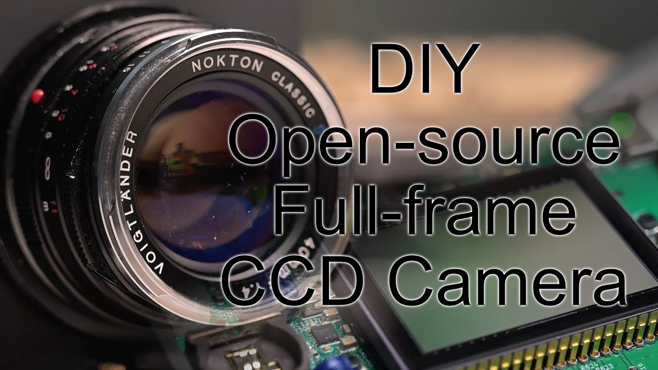
Build a DIY full-frame CCD camera — Wenting Channel

Wenting Channel

Stripping camera architecture down to electronic shutters and digital viewfinders makes custom hardware builds viable, but driving surplus CCD timing registers without vendor documentation introduces analog hurdles an FPGA or CMOS design would avoid.

AI-assisted summary of Build a DIY full-frame CCD camera — original source. Check the original for full context.

Source published:

Key ideas

  • Wenting built an open-source DIY full-frame mirrorless digital camera (Sitina1) around a surplus 11-megapixel Kodak KAI-11000CM interline-transfer CCD and a Leica M mount. (0:00)
  • Driving the multi-phase CCD required pairing an Analog Devices AD9990 front-end with discrete MOSFET drivers and CD4053 multiplexers to overcome vertical clock capacitive loads exceeding 100 pF. (4:06)
  • Readout throughput is hardware-limited to roughly 4.36 FPS at full resolution by the AD9990's 48 MSPS dual-channel ADC, requiring 240p vertical line skipping to achieve a 25 FPS live preview. (8:08)
  • The initial prototype relies entirely on an electronic global shutter, a 4-inch capacitive touchscreen, and a desktop post-processing utility to debayer and export captured RAW frames from an SD card. (11:14)

Detailed notes

## Background Published on YouTube by Wenting Channel on August 15, 2023, this video documents the design and assembly of a functional DIY full-frame CCD digital camera prototype. According to the creator's description, the build is an open-source hobby project (Sitina1 on GitLab) showcasing an initial, imperfect proof of concept that will be refined in future revisions.

## TL;DR Combining a surplus 11-megapixel Kodak KAI-11000CM full-frame CCD sensor with a manual Leica M mount, creator Wenting details the ground-up engineering of an open-source digital mirrorless camera. The architecture pairs an Analog Devices AD9990 analog front-end with an NXP i.MX RT1176 crossover microcontroller, overcoming complex clock-phase driving requirements, discrete level shifting, and hand-soldered PCB assembly. Firmware bring-up involved reverse-engineering undocumented timing registers by hand to stream a live preview to a 4-inch square touchscreen, resolving pipeline challenges like geometric inversion, dual-channel interleaving, debayering, and line-skipping downsampling. Despite prototype limitations—such as off-device PC raw processing, touchscreen shutter triggering, and interactive frame rate bugs—the build successfully captures and stores raw full-frame CCD photographs.

## Atmosphere & style The presentation carries an authentic, understated hacker ethos, characterized by Wenting's refreshingly candid reflections on design missteps, reverse-engineering headaches, and green bodge wires. His methodical, low-key narration balances technical rigor with modest self-deprecation as he shares 'really bad sample photos' and admits where Verilog or a CMOS sensor would have been easier. The pacing feels like an intimate workbench walkthrough, transforming the gritty reality of trial-and-error hardware debugging into a quiet, rewarding milestone when the custom camera finally displays first light.

## Bulletin - [00:00](https://www.youtube.com/watch?v=Ma9FrN5COIo&t=0s) Wenting built an open-source DIY full-frame mirrorless digital camera (Sitina1) around a surplus 11-megapixel Kodak KAI-11000CM interline-transfer CCD and a Leica M mount. - [04:06](https://www.youtube.com/watch?v=Ma9FrN5COIo&t=246s) Driving the multi-phase CCD required pairing an Analog Devices AD9990 front-end with discrete MOSFET drivers and CD4053 multiplexers to overcome vertical clock capacitive loads exceeding 100 pF. - [08:08](https://www.youtube.com/watch?v=Ma9FrN5COIo&t=488s) Readout throughput is hardware-limited to roughly 4.36 FPS at full resolution by the AD9990's 48 MSPS dual-channel ADC, requiring 240p vertical line skipping to achieve a 25 FPS live preview. - [11:14](https://www.youtube.com/watch?v=Ma9FrN5COIo&t=674s) The initial prototype relies entirely on an electronic global shutter, a 4-inch capacitive touchscreen, and a desktop post-processing utility to debayer and export captured RAW frames from an SD card.

## Key takeaways - [00:00](https://www.youtube.com/watch?v=Ma9FrN5COIo&t=0s) To make a DIY digital camera build practical, complex mechanical shutter assemblies and reflex optical viewfinders were replaced with an electronic shutter and an electronic display. - [01:48](https://www.youtube.com/watch?v=Ma9FrN5COIo&t=108s) The Leica M mount was chosen because its short mirrorless flange focal distance accommodates a vast catalog of manual lenses, eliminating the need to reverse-engineer electronic lens protocols. - [01:48](https://www.youtube.com/watch?v=Ma9FrN5COIo&t=108s) Surplus industrial CCDs like the Kodak KAI-11000CM offer publicly accessible datasheets, whereas modern consumer camera sensors typically require restrictive NDAs and industry contacts to acquire. - [04:06](https://www.youtube.com/watch?v=Ma9FrN5COIo&t=246s) The interline-transfer architecture enables a global electronic shutter by shifting photodiode charges into shielded vertical registers, though the reduced light-gathering area lowers full-well capacity. - [04:06](https://www.youtube.com/watch?v=Ma9FrN5COIo&t=246s) Vertical CCD clock pins demand sub-microsecond rise times across capacitive loads exceeding 100 pF, requiring discrete MOSFET driver pairs and CD4053 analog multiplexers for multi-level voltage shifting. - [06:48](https://www.youtube.com/watch?v=Ma9FrN5COIo&t=408s) The prototype PCB functioned reliably despite bypassing high-speed routing conventions like trace length matching and the 3W separation rule on parallel SDRAM lines. - [08:08](https://www.youtube.com/watch?v=Ma9FrN5COIo&t=488s) Configuring the AD9990 timing generator required tedious register reverse-engineering and oscilloscope experimentation due to a total lack of vendor application notes or reference code. - [08:08](https://www.youtube.com/watch?v=Ma9FrN5COIo&t=488s) Raw optical projections from manual prime lenses produce an upside-down image on the sensor plane, requiring an initial 180-degree rotation fix in software. - [08:08](https://www.youtube.com/watch?v=Ma9FrN5COIo&t=488s) Because the KAI-11000CM reads pixels simultaneously outward from both halves of the die, the MCU's CSI peripheral receives an interleaved stream that must be de-interleaved in memory. - [08:08](https://www.youtube.com/watch?v=Ma9FrN5COIo&t=488s) With the dual-channel ADC operating at 48 MSPS aggregate throughput, full 11-megapixel readouts are capped at 4.36 FPS, necessitating vertical line skipping down to 240p for smooth 25 FPS live view. - [11:14](https://www.youtube.com/watch?v=Ma9FrN5COIo&t=674s) Early firmware exhibits an unresolved bug where adjusting the shutter speed alters the live view preview frame rate, and physical triggers were deferred in favor of an on-screen touch button. - [11:14](https://www.youtube.com/watch?v=Ma9FrN5COIo&t=674s) In-camera raw image export was not implemented in the first prototype, instead relying on an off-device desktop utility co-developed with Yukidamayi-san to debayer and develop captured photos.

## Detailed walkthrough ### [00:00](https://www.youtube.com/watch?v=Ma9FrN5COIo&t=0s) DIY Camera Concept and Architecture Simplification

Having practiced DIY electronics for over a decade while actively pursuing photography, Wenting decided it was a natural progression to build a custom digital camera from scratch. Arriving at a functional prototype, he decided to document the engineering and assembly process of this DIY full-frame CCD mirrorless interchangeable-lens camera (MILC), noting that a second video will cover necessary design revisions.

To make the DIY build feasible, the architecture had to be stripped down to the bare essentials: film, shutter, and lens. For a digital build, the physical film is substituted with an image sensor and its supporting drive circuitry. A mechanical shutter presented complex mechanical engineering challenges outside Wenting's expertise, so he opted for an electronic shutter instead.

```mermaid flowchart LR accTitle: Minimalist Digital Camera Architecture accDescr: High-level architectural trade-offs chosen to simplify the DIY camera build. subgraph Simplifications["Design Choices"] A["Film"] -->|"Replace with"| B["CCD Sensor + AFE"] C["Mechanical Shutter"] -->|"Replace with"| D["Electronic Shutter"] E["Optical Viewfinder"] -->|"Replace with"| F["Electronic Viewfinder (DSI Screen)"] end ```

The next challenge was the viewfinder mechanism. A separate side-mounted rangefinder would complicate focusing and focal length changes. An SLR mechanism with reflecting mirrors and prism lenses was also ruled out as far beyond his fabrication skills. Ultimately, he settled on an electronic viewfinder (EVF) using an integrated display for live preview. Although an EVF comes with clear trade-offs—higher power draw, noticeable display latency, and potentially washed-out visibility under direct sunlight—it dramatically simplifies construction while ensuring the preview framing closely reflects the final capture.

- Project repository: open-source on GitLab under `gitlab.com/zephray/Sitina1` - Camera type: DIY full-frame CCD mirrorless interchangeable-lens camera (MILC) - Optical viewfinder alternatives rejected: side rangefinder (focus/zoom parallax issues) and SLR reflex mirror assembly (mechanical complexity)

---

[01:48](https://www.youtube.com/watch?v=Ma9FrN5COIo&t=108s) Component Selection: Sensor, Lens Mount, and Processing Hardware

When choosing parts, lens selection started with the mount interface. To avoid reverse-engineering complex lens communication protocols, Wenting restricted the build to manual glass. Because the mirrorless layout allows for a very short flange focal distance, he chose the Leica M mount, which offers a vast catalog of manual lenses.

Choosing an image sensor was dictated entirely by what appeared on the surplus market. High-end modern camera sensors such as the Sony IMX lineup generally demand non-disclosure agreements (NDAs) to access complete datasheets and remain difficult for hobbyists to acquire. Surplus industrial sensors, however, often have publicly accessible documentation. Wenting acquired several Kodak KAI-11000CM image sensors—an 11-megapixel, 35mm full-frame optical format, interline-transfer CCD capable of global electronic shuttering.

```mermaid flowchart TD accTitle: Hardware Component Interconnect accDescr: Block diagram of core chips, display, power, and sensor interface. subgraph SensorFrontEnd["Sensor Front-End"] CCD["Kodak KAI-11000CM CCD (11MP Full-Frame)"] AFE["Analog Devices AD9990 (AFE + ADC + TG)"] CCD <-->|"Clocks & Dual-channel video"| AFE end

subgraph CoreProcessing["Digital Core"] MCU["NXP i.MX RT1176 MCU"] AFE -->|"CSI Interface"| MCU SDRAM["SDRAM + Flash"] <--> MCU end

subgraph UIandPower["User Interface & Power"] Disp["4-inch 720x720 Capacitive Touchscreen"] Bat["Dual 18650 Battery Pack"] MCU -->|"MIPI DSI"| Disp Bat -->|"Split-rail DC-DC & LDOs"| SensorFrontEnd Bat --> MCU end ```

To drive the CCD, he chose the Analog Devices AD9990, a chip combining an analog front-end (AFE), an analog-to-digital converter (ADC), and an integrated timing generator. For digital control, he selected the NXP i.MX RT1176 crossover microcontroller. Wenting reflected on this architectural choice:

> “I went with this just because I thought it was going to be straightforward (which turned out not to be the case), not because this is the best solution.”

He noted that selecting an all-CMOS sensor path would have bypassed numerous CCD-specific hurdles, just as utilizing an FPGA or an SoC like the AMD/Xilinx Zynq would have delivered higher processing throughput. For user input and display, he paired a 4-inch 720×720 square capacitive touchscreen with the system, eliminating the need to fit mechanical tactile switches into the chassis. The entire system runs on a dual-18650 lithium-ion battery pack.

- Optical sensor: Kodak KAI-11000CM (11 MP, interline-transfer CCD, 35mm full-frame, global electronic shutter) - Sensor controller/AFE: Analog Devices AD9990 (integrated timing generator, analog front-end, ADC) - Main processor: NXP i.MX RT1176 microcontroller - Display: 4-inch 720×720 capacitive touchscreen driven over MIPI DSI - Power source: dual 18650 battery holder modules - Lens mount: Leica M mount (short flange distance, broad manual lens ecosystem)

---

[04:06](https://www.youtube.com/watch?v=Ma9FrN5COIo&t=246s) CCD Physics and Analog Driving Challenges

The digital compute core is straightforward, consisting of the MCU, SDRAM, and flash memory. Driving the CCD, however, proved considerably more difficult. The sensor requires six discrete clock phases to operate. While the AD9990 handles signal generation, amplification, sampling, and digitization with few external components, delivering those signals into the sensor requires specialized driving stages.

Wenting explained how an interline-transfer CCD functions using an illustrative 4×4 pixel array:

```mermaid flowchart TD accTitle: Interline-Transfer CCD Charge Readout Sequence accDescr: Sequence from substrate charge dump to line-by-line serial output. A["1. Electronic Front Curtain: Dump substrate charge"] --> B["2. Exposure: Photons generate electron charge wells"] B --> C["3. Global Transfer: Shift accumulated charge to interline storage columns"] C --> D["4. Vertical Shifting: Toggle vertical clocks to step rows into bottom horizontal buffer"] D --> E["5. Horizontal Readout: Toggle horizontal clocks to shift pixels out to output nodes"] E --> F["6. AFE Conditioning: Buffer, correlate double sample (CDS), amplify, and digitize"] ```

The process begins with an electronic front curtain that purges all residual charge from the substrate. Incoming photons are converted to charge packets across the exposure window. Once exposure concludes, charges transfer simultaneously from the light-sensing photodiode areas into shielded interline vertical shift registers. This simultaneous transfer enables a global electronic shutter. Unlike full-frame architecture CCDs—where the entire silicon footprint gathers light—an interline sensor sacrifices photodiode surface area to fit the vertical storage columns, requiring microlenses above each pixel to refocus light into the narrower collection wells. This smaller collection area diminishes full-well capacity (the saturation charge threshold before blooming occurs), which degrades the sensor's maximum signal-to-noise ratio (SNR).

Once charge packets sit inside the shielded vertical columns, the vertical clocks toggle, stepping an entire row into the horizontal output shift register. High-frequency horizontal clocks then advance pixels one by one out through the charge-to-voltage conversion amplifiers to be sampled.

Bridging the AD9990 to the sensor created heavy analog design challenges. The CCD inputs do not use 3.3V or 5V logic levels: - Vertical clock pins present a massive capacitive load exceeding 100 pF while demanding sub-microsecond rise times ($<1\ \mu\text{s}$). Because standard 74-series logic chips or MCU GPIO pins cannot drive this load, dedicated discrete MOSFET driver pairs were implemented. - Analog multiplexers (CD4053) serve as flexible, multi-level voltage logic level shifters. - Horizontal clocks, having considerably lower input capacitance, are driven using 74-series logic level shifters. - Power rails rely on a combination of split-rail DC-DC converters and linear regulators, though Wenting characterized the initial power circuit design as "actually quite bad" and slated for a complete overhaul in revision two.

---

[06:48](https://www.youtube.com/watch?v=Ma9FrN5COIo&t=408s) PCB Layout, Fabrication, and 3D Printed Prototype Enclosure

The printed circuit board layout was largely an exercise in interconnecting the functional blocks. Because the dual 18650 battery cells dictated a wide footprint, the chassis naturally accommodated the large 4-inch display, giving the PCB plenty of surface area. To keep the overall stack as thin as possible, low-profile board-to-board connectors from Harwin were chosen.

Because this board was intended purely as an experimental proof of concept, Wenting bypassed rigid high-speed routing constraints: - He omitted length matching on the parallel SDRAM traces. - He ignored trace separation rules like the 3W guideline (keeping center-to-center trace separation at three times the trace width to avoid crosstalk), yet the memory interface functioned reliably.

Production files were generated directly from KiCad using the JLCPCB plugin by Benny, and the board was ordered with partial surface-mount assembly (SMT) to accelerate fabrication. Once received, Wenting hand-soldered the remaining parts and debugged the board, leaving several green bodge wires across the circuit.

To test optical alignment and sensor performance, he modeled a quick, modular enclosure and had it 3D printed via JLCPCB's online SLA printing service, avoiding the messy setup and post-processing of a home SLA resin printer.

---

[08:08](https://www.youtube.com/watch?v=Ma9FrN5COIo&t=488s) Firmware Initialization, Timing Registers, and First Light

Firmware development began with the 4-inch MIPI DSI screen, which behaves much like standard SPI or parallel RGB panels: the microcontroller issues an initialization command sequence to configure internal power stages and lookup tables (LUTs) before entering continuous video streaming mode.

Configuring the AD9990 front-end to drive the CCD was significantly more grueling. The chip features dozens of registers to govern exposure, clock phases, and digitization timings, but lacks reference firmware or manufacturer application notes. Wenting had to reverse-engineer the operational registers by studying the raw datasheet:

> “All I can do is read the manual ten times, write down some code, experiment, and then construct the waveform by trial and error. This is taking way longer than I expected. If I were to write some Verilog on FPGA it would take less than a day.”

Once the clock waveforms matched the required timing specifications, the microcontroller's CMOS Sensor Interface (CSI) peripheral was enabled to stream frame data directly into memory and out to the display.

```mermaid flowchart TD accTitle: Raw Data to Display Pipeline and Artifact Corrections accDescr: Corrections applied to raw sensor readout before final display output. Raw["Raw CSI Input: Dual-channel interleaved stream"] A["De-interleave dual channels (Left & Right halves)"] B["Optical inversion correction (180° rotation)"] C["Demosaicing / Debayering (Single-color subpixels to RGB)"] D["Line-skipping subsampling (Reduce to 240p for 25 FPS)"] Final["Corrected 25 FPS Live View Display"]

Raw --> A --> B --> C --> D --> Final ```

Initial test images confirmed optical life, but revealed several image pipeline problems: 1. **Geometric Inversion**: Light passing through a prime manual lens produces an inverted optical projection on the sensor plane, requiring a 180-degree rotation fix in software. 2. **Dual-Channel Interleaving**: The Kodak KAI-11000CM uses dual horizontal readout channels, reading pixels simultaneously from the left and right sides of the die toward outer amplifiers. Because the MCU's CSI peripheral simply dumped the incoming stream sequentially into memory, left-side and right-side pixels were stored alternately, distorting the frame geometry until de-interleaving logic was implemented. 3. **Monochrome Output**: The raw output appeared strictly monochrome. As Wenting explained, outside of specialized 3CCD prisms or Foveon X3 layered-silicon designs, typical camera sensors lack co-located RGB subpixels; individual photodiodes are topped with a single-color Bayer filter mosaic. Producing a color preview requires a software debayering/demosaicing algorithm to interpolate missing color values across neighboring pixels. 4. **Bandwidth Limitations & Frame Rate**: Full-resolution readouts yielded a sluggish refresh rate. The AD9990's ADC samples at 24 MHz per channel, delivering an aggregate 48 megapixels per second across both channels ($24\ \text{MHz} \times 2 = 48\ \text{MSPS}$). Dividing 48 MP/s by the sensor's 11 MP frame size caps the theoretical full-frame readout at roughly 4.3 frames per second: $$\frac{48\ \text{MP/s}}{11\ \text{MP}} \approx 4.36\ \text{FPS}$$ To achieve a smooth 25 FPS live preview, Wenting implemented vertical line skipping. However, because charge packets must be shifted out line by line once a row reaches the horizontal shift register, horizontal pixels cannot simply be dropped mid-row. Consequently, hitting the 25 FPS preview target required downsampling the vertical resolution to 240p.

To handle user adjustments, Wenting built a minimal on-screen touch UI. Although sensor ISO gain sensitivity control was not yet hooked up, manual electronic shutter speed adjustment was fully integrated and functional.

[11:14](https://www.youtube.com/watch?v=Ma9FrN5COIo&t=674s) Touch Controls, Image Processing, and Sample Photos

Wenting demonstrates the camera prototype operating with real-time feedback, though several software and hardware quirks remain in this initial build. There are still lingering bugs in the firmware, most notably an issue where adjusting the shutter speed unintentionally alters the live view frame rate. On the hardware side, the physical shutter button has not yet been mounted to the body, forcing reliance on a software shutter button via the touchscreen interface. As Wenting explains: “I haven’t installed the physical shutter button yet, so the on-screen touch control will do for now.” Tapping the on-screen release actuates the shutter, previews the newly captured image on the display, and commits the raw data onto an onboard SD card.

```mermaid flowchart LR accTitle: Capture and Processing Flow accDescr: Pipeline showing touch capture on camera to SD card storage and PC processing. subgraph Camera["Camera Prototype"] A["Touchscreen Control"] -->|"Triggers capture"| B["CCD Sensor"] B -->|"Previews image"| C["LCD Display"] B -->|"Saves raw data"| D["SD Card"] end subgraph PC["Computer Workflow"] D -.->|"Insert card"| E["PC Utility Tool"] E -->|"Basic image processing"| F["Final Sample Photos"] end ```

Because an in-camera image export pipeline has not been developed yet, getting usable pictures off the system requires popping the SD card out and loading it into a computer. Image conversion relies on a custom helper program running on the desktop: “I haven’t implemented any export feature on the camera, so for now a small utility on PC is used for doing the basic image processing.” Wenting specifically credits collaborator Yukidamayi-san for helping develop this post-processing software tool before sharing what he jokingly terms "some really bad sample photos." Concluding the overview of the first prototype's progress, Wenting promises that the next installment will dig deeper into UI refinements, further system improvements, higher-quality photos, and behind-the-scenes engineering anecdotes before signing off to read viewer thoughts in the comments.

- **Current Software Bugs**: Changing the shutter speed setting directly alters the frame rate of the live view feed. - **Workflow & Processing**: - Shutter triggering is currently handled via capacitive/resistive touch controls on the display. - Images are captured, flashed onto the screen for confirmation, and written straight to SD storage. - Raw sensor frames are converted and processed off-device using a bespoke PC utility created with help from Yukidamayi-san. - **Upcoming Developments**: Future coverage will focus on physical refinements, user interface development, better photo samples, and behind-the-scenes development stories.

## Mentioned Wenting, Yukidamayi-san, Benny, Kodak KAI-11000CM, Analog Devices AD9990, NXP i.MX RT1176, Leica M mount, JLCPCB, Harwin, KiCad, GitLab, CD4053, Sony IMX, AMD/Xilinx Zynq

## Video description Just something I have been working on recently for fun. This is the first prototype so it's quite broken now. Still need to improve lot of the aspects. The project is open source on gitlab.com/zephray/Sitina1. Order your PCB at www.jlcpcb.com.

[Source](https://www.youtube.com/watch?v=Ma9FrN5COIo)

中文简报

Wenting基于柯达库存芯片打造开源全画幅CCD相机 将相机架构精简至电子快门和电子取景器使自制硬件变得可行,但在缺乏原厂文档的情况下驱动库存CCD时序寄存器,带来了FPGA或CMOS设计本可避免的模拟电路难题。 创作者Wenting将一块1100万像素的柯达KAI-11000CM全画幅CCD库存传感器与徕卡M手动卡口相结合,详尽展示了一款开源微单数码相机的从零开发过程。该架构将亚德诺半导体(Analog Devices)AD9990模拟前端与恩智浦(NXP)i.MX RT1176跨界微控制器相搭配,克服了复杂的时钟相位驱动要求、分立电平转换以及手工焊接PCB的装配挑战。固件调试阶段通过手动逆向未公开的时序寄存器,实现了在4英寸方形触摸屏上的实时预览流传输,并解决了诸如几何反转、双通道交织、去马赛克以及跳行下采样等处理管线难题。尽管原型机仍存在一些局限——例如需在PC端进行RAW格式后处理、通过触摸屏触发快门以及交互帧率缺陷——该设备依然成功拍摄并保存了全画幅RAW格式CCD照片。 Wenting围绕一块库存的1100万像素柯达KAI-11000CM行间转移CCD和徕卡M卡口,打造了一款开源DIY全画幅微单数码相机(Sitina1)。 (0:00) 驱动多相CCD需要将亚德诺半导体AD9990前端与分立MOSFET驱动器及CD4053多路复用器配合使用,以克服超过100 pF的垂直时钟容性负载。 (4:06) 由于AD9990的48 MSPS双通道ADC限制,全分辨率下的读取吞吐量受硬件制约约为4.36 FPS,需要通过240p垂直跳行来达到25 FPS的实时取景预览。 (8:08) 最初的原型机完全依赖电子全局快门、一块4英寸电容触摸屏,以及桌面端后处理实用程序来对SD卡中捕获的RAW帧进行去马赛克和导出。 (11:14)

Reading summary

Wenting documented the engineering of a functional DIY full-frame mirrorless digital camera built around an 11-megapixel surplus Kodak CCD, balancing extreme mechanical simplification against complex analog driving circuitry and register reverse-engineering. Minimalist Architecture and Surplus Hardware (0:00) To make a scratch-built digital camera feasible, Wenting stripped the mechanical design down to bare essentials. He replaced physical focal-plane shutters with an electronic shutter and substituted optical viewfinders—which would require complex SLR reflex mirrors or parallax-prone rangefinder mechanics—with an electronic viewfinder powered by a 4-inch 720×720 capacitive touchscreen. To avoid reverse-engineering proprietary lens communication protocols, he selected the Leica M mount, taking advantage of its short flange focal distance and vast ecosystem of manual lenses. Sensor selection was dictated by the surplus electronics market. While modern CMOS sensors like Sony's IMX series require restrictive non-disclosure agreements to obtain datasheets, surplus industrial chips provide publicly accessible documentation. Wenting acquired Kodak KAI-11000CM sensors, an 11-megapixel 35mm full-frame interline-transfer CCD capable of global electronic shuttering. For the compute and mixed-signal core, he paired an Analog Devices AD9990 analog front-end (AFE) and timing generator with an NXP i.MX RT1176 crossover microcontroller, powered by dual 18650 lithium-ion cells. Wenting noted this was chosen for anticipated simplicity rather than optimal throughput, acknowledging that an FPGA or modern CMOS sensor would have bypassed significant analog hurdles. Analog Drive Demands and CCD Physics (4:06) Operating the Kodak CCD presented severe analog engineering demands. Unlike CMOS sensors with integrated drive logic, the interline-transfer CCD requires six discrete clock phases and non-standard voltage levels. The vertical clock pins present a capacitive load exceeding 100 pF while demanding rise times under one microsecond. Standard logic ICs or microcontroller GPIOs cannot drive this load, compelling Wenting to construct dedicated discrete MOSFET driver pairs alongside CD4053 analog multiplexers configured as multi-level logic level shifters. Horizontal clocks, having lower capacitance, were driven via 74-series level shifters. The sensor's interline architecture underpins both its functionality and physical trade-offs. To implement an electronic global shutter, the chip executes an electronic substrate charge dump, integrates incoming photons, and simultaneously shifts accumulated charges from photodiodes into shielded vertical shift registers. These registers incrementally step rows into a horizontal readout buffer. However, allocating die surface to shielded storage columns reduces light-gathering photodiode area, diminishing full-well capacity and lowering the maximum signal-to-noise ratio compared to full-frame transfer CCDs. Timing Reverse-Engineering and Sensor Pipeline (8:08) Firmware configuration of the AD9990 front-end proved to be the project's most grueling software bottleneck. Lacking manufacturer reference code or application notes, Wenting spent extensive time interpreting raw datasheets to configure dozens of registers governing exposure, phase clocks, and digitization timings by trial and error—a process he estimated would have taken under a day in Verilog on an FPGA. Once digitized, raw sensor data required multi-stage algorithmic correction before display. Because the Kodak KAI-11000CM reads out through dual horizontal channels—shifting left and right frame halves toward outer amplifiers simultaneously—the microcontroller's CMOS Sensor Interface (CSI) initially dumped interleaved pixels sequentially into memory, requiring de-interleaving logic. The software also applied a 180-degree geometric rotation to correct optical lens inversion and executed demosaicing algorithms across the Bayer color filter array. Furthermore, because aggregate ADC bandwidth is capped at 48 MSPS (24 MHz across two channels), full 11 MP readout is physically limited to roughly 4.36 frames per second. To achieve a 25 FPS live preview, Wenting implemented vertical line skipping down to 240p, as individual horizontal pixels cannot be dropped once a row enters the shift register. Prototype Fabrication, Firmware Bugs, and Processing (11:14) Hardware assembly relied on pragmatic shortcuts. For the custom PCB, Wenting omitted length matching on parallel SDRAM traces and bypassed 3W trace-separation guidelines, yet the memory subsystem functioned reliably. The board was ordered partially assembled from JLCPCB and hand-finished with several bodge wires, housed in a rapid SLA 3D-printed enclosure. In its initial functional state, the prototype exhibits several software and hardware constraints. Shutter actuation relies entirely on an on-screen touch button because a physical shutter release has not yet been mounted. Additionally, a firmware glitch causes adjustments to electronic shutter speed to unintentionally alter the live view frame rate. Because on-camera export pipelines were omitted, raw captured frames are saved directly to an SD card and transferred to a computer, where a bespoke desktop utility co-developed with Yukidamayi-san handles final image processing. Wenting treats this initial build as an experimental proof of concept demonstrating the feasibility of a DIY digital camera, noting that its power rail design is inefficient and slated for replacement. A planned second revision aims to overhaul the power circuitry, resolve live-view frame-rate bugs, install physical shutter buttons, and improve optical results.

精炼阅读摘要

硬件开发者Wenting基于开源项目Sitina1,从零设计并制作了一台全画幅CCD无反可换镜头相机原型机。该项目用工业库存CCD芯片、电子快门和触控屏电子取景器替代胶片、机械快门与光学反光镜,在规避高难度精密机械加工的同时验证了自制数码相机的可行性。 极简架构权衡与核心元器件选型 (0:00) 为了让自制数码相机具备可行性,Wenting将系统结构简化为感光元件、快门与镜头三大核心要素。机械快门、单反反光板与旁轴测距仪涉及极高的精密机械加工门槛,因而被全面弃用;取景方案选用了基于4英寸720×720 MIPI DSI电容触控屏的电子取景器(EVF),虽然存在功耗上升、显示延迟和强光下可视性差的劣势,但大幅降低了物理制作复杂度。镜头卡口选用无反法兰距极短的徕卡M卡口,直接利用成熟庞大的手动镜头群,免去了逆向解析镜头自动通信协议的难题。 核心传感器受限于公开市场渠道,索尼IMX等现代传感器因非公开数据手册及保密协议限制难以获取,Wenting最终选用工业剩余市场中的柯达KAI-11000CM——一款1100万像素、35mm全画幅的行间转移型(Interline-transfer)CCD,具备公开技术文档并支持全局电子快门。模拟前端选用集成定时发生器、ADC与放大器的ADI AD9990,数字主控采用恩智浦i.MX RT1176微控制器,整机由双18650锂电池供电。Wenting坦言,选择MCU驱动CCD在开发中遇到了预期之外的困难,若选用CMOS传感器或FPGA/Zynq平台,系统带宽和实现难度本会更具优势。 行间转移CCD原理与模拟驱动难点 (4:06) 相较于由微控制器、SDRAM和闪存构成的常规数字核心,CCD的模拟驱动设计构成了最大的工程挑战。KAI-11000CM采用行间转移架构,曝光周期始于电子前帘衬底电荷清空,光电二极管将光子转化为电荷包后,在曝光结束瞬间全局同步转移到带有光学屏蔽的垂直移位寄存器中,从而实现全局电子快门。但由于垂直寄存器挤占了有效感光面积,必须通过微透镜聚光,这不可避免地降低了满阱容量并削弱了传感器的最大信噪比。 在电气接口层面,驱动该CCD需要6个离散时钟相位,且垂直时钟引脚呈现出超过100 pF的巨大电容负载,要求上升时间低于1微秒。常规74系列逻辑门芯片或单片机GPIO完全无法驱动,Wenting专门设计了分立MOSFET驱动对,并配合CD4053模拟多路复用器作为多电平逻辑电平转换器;输入电容较小的水平时钟则采用74系列电平转换芯片。供电部分依赖多轨分立DC-DC转换器与LDO组合,但Wenting评价初版电源电路设计表现较差,计划在第二版中全面推倒重做。 硬件PCB布局与外壳快速成型 (6:48) 在印刷电路板设计上,双18650电池仓的占位奠定了相对宽大的机身布局,该物理宽度恰好可以容纳4英寸正方形触控屏,并为单板提供了充足的布线空间。为了最大限度降低堆叠厚度,电路板互连选用了Harwin超薄板对板连接器。 作为概念验证原型,Wenting在高速布线规则上采取了实用主义的折中策略:并行SDRAM总线没有进行等长匹配,同时也忽略了防止串扰的3W走线间距规则,但实测存储系统仍能稳定运行。PCB通过KiCad搭配JLCPCB插件生成生产文件并采用部分SMT贴片代工,收板后手工焊接剩余元器件并飞线排错。机身外壳经快速建模后采用第三方SLA光固化3D打印服务制作,避免了个人在工作间处理光敏树脂的复杂后处理流程。 固件时序逆向与图像管线构建 (8:08) 固件开发中,屏幕初始化相对标准化,但AD9990前端芯片完全缺乏官方参考代码或应用笔记。Wenting只能通过反复精读数据手册并以试错法编写寄存器,逆向配置驱动CCD所需的时钟波形,其调试耗时远超预估。当通过MCU的CSI接口将原始数据流导入内存后,图像管线暴露出一系列物理与数据缺陷:镜头光路成像上下颠倒,需在软件中执行180度几何旋转;CCD采用左右双通道水平读出机制,直接存入内存会导致画面左右两侧像素交错混杂,必须编写去交错算法恢复空间排列;传感器表面的拜耳滤镜原始输出仅为灰度数据,需通过去马赛克算法插值计算色彩。 此外,系统遭遇了严重的读出带宽瓶颈。AD9990的双通道ADC采样率为单通道24 MHz,整机吞吐量为48 MSPS,除以1100万像素后理论全幅刷新率仅约4.36 FPS。为获得25 FPS的实时流畅取景,固件采用了垂直跳线采样,将实时预览分辨率降至240p。拍摄控制方面,目前依赖触控屏软按键触发快门并写入SD卡,但调节快门速度会导致实时画面帧率异常变化;机内图像导出功能尚未开发,RAW格式转换暂时依赖协作者Yukidamayi-san编写的PC端小工具完成。 该原型机成功打通了全画幅CCD在无反架构下的成像全流程,但仍存在机内无法直接导出成片、快门调节牵动预览帧率、缺少实体快门键以及电源与模拟驱动底噪较大等问题。Wenting表示将在第二代设计中重构电源管理电路、优化用户界面并完善机械结构。

Detailed notes — zh

## Background 该视频由 Wenting Channel 于 2023 年 8 月 15 日发布在 YouTube 平台上。视频简介说明这是作者近期出于兴趣制作的自研全画幅 CCD 相机初代工程样机,目前仍存在不少缺陷且亟待完善,整个项目已在 GitLab(GitLab.com/zephray/Sitina1)完全开源,并推荐通过 JLCPCB 进行 PCB 打样制造。 ## TL;DR 视频记录了作者 Wenting 独立设计并制造全画幅微单数码相机(Sitina1)完整硬件原型的历程。作者采用极简架构思路,省去机械快门与复杂光学反光系统,选用柯达 1100 万像素全画幅 CCD 传感器(KAI-11000CM)、ADI AD9990 模拟前端驱动器、NXP i.MX RT1176 跨界主控,并搭配徕卡 M 卡口与方形触摸屏。在硬件实现上,作者攻克了高压多轨供电、大电容负载垂直时钟推挽驱动、示波器逆向寄存器时序调试等重重难关;在软件与成像端,则通过解决图像翻转、双通道交错重组以及 Bayer 去马赛克算法成功重现全彩图像,并利用垂直抽行将预览刷新率提升至可用的 25FPS。最后,作者展示了触控触发拍摄、写入 SD 卡并在 PC 工具处理后得到的首批实拍样片,同时预告了下一期的系统改进计划。 ## Atmosphere & style 整期视频散发着纯粹、硬核且极其扎实的个人极客工程美学,叙事语调平静务实、客观坦率。作者毫无保留地将研发过程中的狼狈与真实试错摆在台前——从缺少技术文档只能死啃芯片手册十遍的无力感,到满板飞线与简易 3D 打印外壳的粗粝质感,再到开机时面对畸变黑白画面的逐层破案,既充满自嘲调侃,又洋溢着硬件调通瞬间那种难以掩饰的成就感。观看体验如同在深夜的工作台前,屏息凝神地见证一位硬核创作者用烙铁、示波器与底层代码,从零手搓出一台真正能拍照的现代相机的硬核冒险。 ## Bulletin - [00:00](https://www.youtube.com/watch?v=Ma9FrN5COIo&t=0s) Wenting 开源了名为 Sitina1 的 DIY 全画幅微单相机项目,选用 1100 万像素柯达 KAI-11000CM 隔行传输 CCD,原生支持电子全局快门,搭配徕卡 M 卡口手动镜头群以规避自动对焦协议逆向及机械快门设计。 - [03:53](https://www.youtube.com/watch?v=Ma9FrN5COIo&t=233s) 核心电路由 ADI AD9990(时序发生器/AFE/ADC)与 NXP i.MX RT1176 跨界主控构成,通过 CD4053 与大电流 MOSFET 推挽电路攻克了 CCD 垂直时钟大容性负载(>100pF)与微秒级高压驱动难题。 - [10:26](https://www.youtube.com/watch?v=Ma9FrN5COIo&t=626s) 受限于双通道 48MSPS 的读出吞吐瓶颈,11MP 全像素读出理论帧率仅约 4.3 FPS;因 CCD 水平移位寄存器无法行内跳点,取景预览只能通过垂直抽行将分辨率压缩至 240p,强行拉升至 25 FPS 流畅度。 - [11:14](https://www.youtube.com/watch?v=Ma9FrN5COIo&t=674s) 初代原型机已实现触屏交互、电子快门控制、图像实时解交错与去马赛克回显,并能将 RAW 数据写入 SD 卡,借助 PC 端配套工具完成基础图像后处理导出。 ## Key takeaways - [00:00](https://www.youtube.com/watch?v=Ma9FrN5COIo&t=0s) 相机构架推行极致减法原则:选用图像传感器替代胶片,以电子快门取代高精密的机械快门帘幕组件,规避机械磨损与设计难度。 - [00:45](https://www.youtube.com/watch?v=Ma9FrN5COIo&t=45s) 放弃结构复杂的旁轴与单反光学取景系统,采用 4 英寸 720×720 方形触控屏构建电子取景器(EVF),换取“所见即所得”与免打实体按键孔的便利。 - [01:48](https://www.youtube.com/watch?v=Ma9FrN5COIo&t=108s) 因商业 CMOS 数据手册受 NDA 严密保护,最终从二手渠道采购工业拆机柯达 KAI-11000CM 隔行传输 CCD,天生具备硬件全局快门特性。 - [01:48](https://www.youtube.com/watch?v=Ma9FrN5COIo&t=108s) 选用短法兰距的徕卡 M 手动镜头卡口,彻底避开现代自动对焦镜头极其繁琐的底层通信协议逆向工程。 - [03:53](https://www.youtube.com/watch?v=Ma9FrN5COIo&t=233s) 隔行传输 CCD 依赖感光单元旁的遮光存储列实现全局曝光,但感光面积缩减导致满阱容量下降,限制了最大信噪比(SNR)。 - [05:45](https://www.youtube.com/watch?v=Ma9FrN5COIo&t=345s) CCD 垂直时钟引脚容性负载超过 100pF 且要求上升时间小于 1µs,单片机 IO 无法直推,需采用专用推挽电路与 CD4053 搭建电平转换驱动。 - [08:05](https://www.youtube.com/watch?v=Ma9FrN5COIo&t=485s) 缺乏应用笔记与参考代码,AD9990 复杂寄存器配置完全依赖示波器与面包板盲测逆向调试,耗时远超初期预期。 - [06:48](https://www.youtube.com/watch?v=Ma9FrN5COIo&t=408s) 通过 KiCad JLCPCB 插件完成打样与基础贴片,未对 SDRAM 进行严苛等长匹配或 3W 高频走线规则,系统仍实现稳定运行。 - [07:15](https://www.youtube.com/watch?v=Ma9FrN5COIo&t=435s) 利用外包 3D 打印快速成型临时验证外壳,免去了个人在室内维护树脂光固化(SLA)打印机的脏污麻烦。 - [09:08](https://www.youtube.com/watch?v=Ma9FrN5COIo&t=548s) 针对双通道同时输出导致的数据交叉错乱,固件必须重构左右像素内存拓扑,并依次叠加几何反转与 Bayer 去马赛克算法还原色彩。 - [10:26](https://www.youtube.com/watch?v=Ma9FrN5COIo&t=626s) 双通道 ADC 转换上限为 48MP/s,直读 11MP 图像仅能达到 4.3 FPS,无法支撑基础的取景器交互需求。 - [11:02](https://www.youtube.com/watch?v=Ma9FrN5COIo&t=662s) CCD 物理结构决定了水平像素无法中途跳读,提升实时帧率只能牺牲垂直分辨率,通过大幅抽行压至 240p 实现 25 FPS 取景。 - [11:14](https://www.youtube.com/watch?v=Ma9FrN5COIo&t=674s) 初代原型机已调通电子快门时钟脉冲调节,但尚未实装硬件快门实体键,拍摄触发暂时完全交由电容触控屏完成。 - [11:40](https://www.youtube.com/watch?v=Ma9FrN5COIo&t=700s) 样机暂未集成复杂的机内 JPEG 压缩与导出功能,拍摄数据以原始格式直存 SD 卡,依托 PC 端轻量级工具完成最终后处理生成样张。 ## Detailed walkthrough ### [00:00](https://www.youtube.com/watch?v=Ma9FrN5COIo&t=0s) DIY 全画幅微单的构想与极简架构设计 Wenting 拥有十多年的电子 DIY 经验,同时也是一名摄影爱好者,因此亲手打造一台属于自己的相机对他来说是一个水到渠成的想法。经过一段时间的研发,他终于做出了可以公开展示的初代原型机(开源项目代号为 Sitina1),并在本期视频中详细拆解整个设计与制作过程。由于目前的工程样机还处于初期阶段、存在不少缺陷,后续还将推出 Part 2 来展示改进方案。在整体架构构思上,DIY 的核心原则就是“极度简化”。一台相机最基础的要素无非是“胶片、快门和镜头”三样东西:在数码时代,胶片被图像传感器及其外围电路替代;机械快门结构极其精密复杂,由于机械设计并非 Wenting 的强项,他直接采用电子快门予以省除。 做完减法后,机器虽然能够感光拍照,但还缺少取景器。Wenting 权衡了三种取景方案:第一种是像旁轴相机那样加装光学旁轴测距取景器,但这会给变焦和精确对焦带来巨大麻烦;第二种是做成单反结构(SLR),依赖反光镜和五棱镜/五面镜,虽然光学效果出色,但其极其复杂的机械构造早已远远超出个人制造的能力范围;第三种则是最现实的方案——电子取景器(EVF),直接利用屏幕显示图像预览。尽管电子屏幕取景存在功耗高、延迟大、在强烈阳光下户外可见度差等缺点,但它不仅实现门槛最低,还能做到“所见即所得”,预览画面与成片高度一致。为了让设计保持简单,Wenting 毫不犹豫地选择了电子取景方案。 ```mermaid flowchart TD accTitle: 核心架构极简化推演 accDescr: 展示作者如何将传统相机的机械部件一步步替换为电子元器件以降低DIY门槛 subgraph Traditional["传统相机三要素"] direction TB T1["胶片 (Film)"] T2["机械快门 (Shutter)"] T3["镜头 (Lens)"] end subgraph Modern["Sitina1 极简设计替代"] direction TB M1["图像传感器 + AFE 电路"] M2["全电子快门 (省去复杂机械)"] M3["手动镜头 + Leica M 卡口"] end subgraph VF["取景方案决策"] direction TB V1["旁轴取景 (变焦对焦难)"] -.->|放弃| V3["电子取景器 EVF / 屏幕"] V2["单反反光镜 (机械难度超标)"] -.->|放弃| V3 end T1 ==> M1 T2 ==> M2 T3 ==> M3 M1 --> V3 ``` - **开源项目地址**:GitLab 上的 `gitlab.com/zephray/Sitina1`。 - **电子快门策略**:彻底规避机械快门帘幕组件的公差与磨损问题。 - **电子取景代价**:换取了“所见即所得”的易用性,但承担了高功耗、画面延迟及强光可见度低的硬件成本。 --- ### [01:48](https://www.youtube.com/watch?v=Ma9FrN5COIo&t=108s) 核心元器件选型:M卡口、柯达CCD与跨界主控 器件选型的第一项是镜头与卡口。为了避免耗费海量精力去逆向工程现代自动对焦镜头的通信协议,选择纯手动镜头是最合理的路径。鉴于这是一台无反微单相机(MILC),法兰距可以做得很短,Wenting 决定选用拥有庞大手动镜头群的徕卡 M 卡口(Leica M-mount)。在图像传感器(Sensor)的选型上,自由度则被现实狠狠压缩:“传感器实际上轮不到我挑三拣四,二手市场上能淘到什么我就只能用什么。”相机行业常见的索尼 IMX 系列 CMOS 虽然性能极其出色,但厂商通常需要签署严苛的保密协议(NDA)才肯开放完整数据手册(Datasheet),个人渠道极难买到。另一种途径是寻找工业相机拆机的图像传感器,往往能找到公开的数据手册。Wenting 非常幸运地淘到了一批柯达(Kodak)KAI-11000CM 传感器,这是一款拥有 1100 万像素、采用 35mm 全画幅光学规格的隔行传输型 CCD(Interline Transfer CCD),天生支持全局电子快门。 为了驱动这枚全画幅 CCD,Wenting 选用了来自 Analog Devices(ADI)的 AD9990,这是一颗集成了时序发生器(Timing Generator)、模拟前端(AFE)以及 ADC 的高度集成驱动芯片。在主控处理器方面,他选用了 NXP 的高性能跨界单片机 i.MX RT1176。Wenting 直言,其实完全有更省事的方案,比如直接用 CMOS 传感器能省去绝大多数麻烦,或者在 CCD 方案中采用 FPGA 生成驱动时序、甚至用 Xilinx Zynq 这种 SoC FPGA 来获取更好的吞吐性能:“我选择这套方案纯粹是因为我一开始以为它会比较简单直接(结果证明根本不是那么回事),而不是因为它是最优解。”在显示端,为了保证高像素密度(PPI),他挑选了一块 4 英寸、分辨率为 720×720 的电容触摸屏,这样还顺便省去了在机身开孔布置实体按键的机械结构困扰;供电则采用两节标准的 18650 锂电池模块。 - **图像传感器**:Kodak KAI-11000CM(11MP 全画幅 35mm 隔行传输 CCD,原生支持电子全局快门)。 - **模拟前端驱动器**:ADI AD9990(集成 CCD 时序发生器、AFE 与高速 ADC)。 - **主控制器**:NXP i.MX RT1176 跨界微控制器。 - **镜头卡口**:Leica M 卡口(短法兰距、纯手动操作无需协议逆向)。 - **显示与交互**:4 英寸 720×720 方形高 PPI 屏幕,集成电容式触控面板。 - **电源供应**:双节 18650 电池组模块。 --- ### [03:53](https://www.youtube.com/watch?v=Ma9FrN5COIo&t=233s) CCD 工作原理解析与严苛的高压时序驱动电路 相机的电路主要分为处理部分与传感器驱动部分。处理器周边相当常规,仅包含主控芯片、RAM 和闪存。而柯达 CCD 的驱动难度极大,光是维持基本运转就需要 6 路不同的时钟信号。AD9990 的优势在于单芯片集成:一侧向 CCD 发出所需的各类驱动时钟,另一侧直接捕获 CCD 输出的微弱模拟信号,并在芯片内部完成放大、相关双采样(CDS)与模数转换。 为了解释为什么需要这些信号,Wenting 以一个简化的 4×4 阵列详细演示了隔行传输 CCD(Interline Transfer CCD)的感光与读出机制: 1. **电子前帘复位**:启动时,电路发出脉冲清空器件上残留的所有寄生电荷; 2. **曝光感光**:光线照射在感光元件上,转换为与曝光量成正比的电荷; 3. **电荷转移(全局快门)**:曝光结束的瞬间,所有感光像素中累积的电荷被同步转移到相邻的遮光存储区(Storage Element),这正是硬件全局快门的物理实现机制。“隔行传输”之名即源于感光列与垂直电荷转移列相互交错的布局。与其对应的概念是“全画幅 CCD”(Full-frame CCD,此处指传感器内部物理结构而非 35mm 画幅尺寸),后者的感光面百分之百用来感光,没有内置遮光存储列,必须依赖机械快门挡光来读出。隔行传输 CCD 虽然省去了机械快门,但感光面积缩减导致其必须依靠微透镜(Microlens)把光线聚集到狭窄的感光窗口中,这直接减少了满阱容量(Full Well Capacity),限制了传感器溢出前能容纳的最大电荷量,进而降低了最大信噪比(SNR); 4. **垂直与水平移位读出**:电荷转移到存储区后,芯片触发垂直时钟(Vertical Clock),将最底部的整行像素电荷推入底部输出缓冲寄存器;随后触发高速水平时钟(Horizontal Clock),将这行像素一个挨一个地平移推送到输出引脚,送入模拟前端进行缓冲、放大并数字化。 ```mermaid flowchart LR accTitle: 隔行传输 CCD 读出流程 accDescr: 说明感光、电荷转移至存储单元以及垂直和水平时钟如何协同将像素送出 subgraph Exposure["1. 曝光与转移"] direction TB E1["电子前帘复位清空余电"] --> E2["感光元件光电转换"] E2 -->|"全局快门脉冲"| E3["瞬间转入隔行存储列"] end subgraph Transfer["2. 行列逐级移位"] direction TB T1["垂直时钟 (Vertical Clocks)"] -->|"整行下推"| T2["水平输出寄存器"] T3["水平时钟 (Horizontal Clocks)"] -->|"单像素平移"| T4["模拟信号输出端"] T2 --> T4 end subgraph Readout["3. 模数处理 (AD9990)"] direction TB R1["缓冲与低噪声放大"] --> R2["相关双采样 (CDS)"] R2 --> R3["ADC 数字化为 RAW 数据"] end Exposure --> Transfer Transfer --> Readout ``` 在硬件实现上,虽然 AD9990 能够产生这些逻辑时序,但 CCD 的引脚完全无法接受常规的 3.3V 或 5V 逻辑电平。这导致硬件电路面临极大的供电与电平驱动挑战: - **电源轨复杂而混乱**:传感器需要多个正负不一的高压轨。Wenting 在板上使用了多路分离轨(Split-rail)DC-DC 开关电源芯片与低压差线性稳压器(LDO)。Wenting 坦白承认这里的硬件设计相当粗糙,电源拓扑并不理想,留待后续版本重构。 - **驱动电平极其苛刻**:垂直时钟引脚不仅需要高摆幅电压,还呈现出超过 100pF 的大容性负载,同时要求上升时间必须小于 1 微秒(< 1µs)。这种瞬态充放电能力远远超出了普通单片机或 74 系列逻辑 IC 的 IO 驱动极限。为此,Wenting 在垂直时钟线路上采用了专用大电流 MOSFET 搭建推挽电路,并使用 CD4053 模拟多路复用芯片充当通用电平转换器;相比之下,水平时钟引脚的寄生电容负载要小得多,因此可以直接通过 74 系列逻辑芯片搭配电平移位电路进行驱动。 --- ### [06:48](https://www.youtube.com/watch?v=Ma9FrN5COIo&t=408s) PCB绘制、3D打印机壳与波形调试的漫长折磨 进入 PCB 布局阶段,Wenting 发现由于选用了大容量的双 18650 电池,屏幕相应地也必须选得比较大,这反而在 PCB 上留出了宽裕的走线空间。为了在容纳大尺寸元器件的同时把整机厚度压缩到极致,他在电路板连接器上选用了 Harwin 的低矮型连接件。作为用于技术验证的实验工程板,他在高速数字布线时并未过分纠结于细节:板载 SDRAM 的走线既没有进行严格的等长匹配,也没有遵循高频走线的 3W 规则,“但它依然稳定工作了”。他利用 KiCAD 的 JLCPCB 插件一键导出生产制造文件,连同部分贴片(PCBA)组装服务直接交付工厂加工。拿到回板后,他手工补焊了剩余的分立元器件,板面上也留下了不少后期调试跳线(Bodge wires)的痕迹。 机壳方面,Wenting 强调目前看到的只是一个用来快速配合镜头验证成像系统的简易外壳,远非最终产品形态。他直接调用了三维打印服务定制外壳,彻底省去了在家里调试光固化(SLA)树脂打印机产生的各种脏乱困扰。 机壳拼装前必须先跑通底层固件。软件适配工作从简到繁: - **MIPI DSI 屏幕驱动**:这一部分较为简单。与其他常见的并行或 SPI 屏幕类似,通过初始化序列依次写入供电配置、查找表(LUT)等参数,随后将控制器切入 Video 模式即可像驱动标准 RGB 屏一样显示画面。 - **CCD 寄存器逆向摸索**:这是整个项目最痛苦的攻坚阶段。虽然 AD9990 芯片功能强大、寄存器配置极其丰富,但 Wenting 手头除了一份枯燥简略的数据手册外,既没有任何厂商应用笔记(Application Note),也没有任何参考示例代码。“我唯一能做的就是把手册前前后后硬读十遍,自己写出驱动代码,在面包板与示波器上不断实验,通过一次次的试错去手动拼接时序波形。”Wenting 无奈地感慨道:“这花费的时间远远超出了我的预期。如果当初直接用 FPGA 写 Verilog 来生成这些时序,可能连一天都用不上。”历经无数次寄存器试错调试,示波器上终于捕获到了精确的波形,主控 i.MX RT 的 CMOS 传感器接口(CSI)被成功使能。当他在裸露的传感器感光面上放上一个小物体时,屏幕上终于映出了传感器的首批灰度光影。 --- ### [09:08](https://www.youtube.com/watch?v=Ma9FrN5COIo&t=548s) 图像还原的“破案现场”:翻转、双通道交错与去马赛克 为了真正当成相机拍照,Wenting 迅速把传感器装进了 3D 打印的临时机壳并拧上镜头。然而,开机预览呈现出来的第一幅画面极其诡异:全屏不仅是单色黑白画面,方向完全颠倒,且画面尺寸与比例也完全错乱。Wenting 随即在固件中展开了逐层“破案”与画面重构: ```mermaid flowchart TD accTitle: CCD 原始图像还原处理管线 accDescr: 展示如何将颠倒、交错的原始传感器输出转换为正确的彩色预览图像 Raw["CCD 原始数据流"] --> Inverse["1. 画面几何反转 (修复光学镜头倒立成像)"] Inverse --> Deinterleave["2. 左右通道解交错 (修复左右同时读出导致的内存穿插)"] Deinterleave --> Debayer["3. Bayer 去马赛克算法 (单像素插值恢复RGB全彩)"] Debayer --> Final["正确显示的彩色实时预览画面"] ``` 1. **画面颠倒**:光线通过镜头光学镜片组后会在焦平面上投射出倒立实像,处理逻辑只需进行一次简单的镜像/反转映射即可复位。 2. **画面拉伸撕裂与尺寸畸变**:KAI-11000CM 传感器为了提高读出速度,采用了“双通道读出”架构(Dual-channel Readout),即传感器的左半区域与右半区域分别由两个独立的输出端口同时向外推送数据。然而,后级处理器的 CSI 控制器并不了解传感器的物理分块机制,只是机械地按照输入时钟顺序将左右通道的数据交替存入内存。如果在屏幕上直接按内存线性地址顺序刷出,左半边像素和右半边像素就会死死穿插在一起,导致整幅图像被完全割裂。必须通过软件算法重新将左右交替的数据拆开并拼接回正确的空间拓扑。 3. **缺少色彩(黑白马赛克)**:Wenting 解释道,许多人常识中认为每个像素都由红、绿、蓝(RGB)三个子像素构成,但除适马 Foveon X3 三层感光元件或特殊的 3CCD 棱镜系统外,绝大多数单传感器相机在物理上根本没有子像素结构。每个感光单元上方仅覆盖了一片特定颜色的微型滤光片(即拜耳滤镜阵列 Bayer Filter),单个像素物理上只能记录一种颜色的光强。色彩的还原完全依赖软件后期的去马赛克(Debayering)算法,根据邻近像素的光强插值计算出每个像素缺失的另外两种颜色分量。 将反转算法、通道解交错算法与拜耳插值算法全部融合后,屏幕上终于呈现出色彩正常、比例正确的全画幅实时画面。 --- ### [10:26](https://www.youtube.com/watch?v=Ma9FrN5COIo&t=626s) 吞吐瓶颈下的抽行折衷与基础 UI 开发 色彩和画面几何形态虽然修复完毕,但整个实时取景系统陷入了极具挫败感的卡顿之中,帧率低得犹如幻灯片。Wenting 现场进行了数据吞吐率的底线测算: - 传感器总像素高达 1100 万像素(11MP); - AD9990 的 ADC 转换时钟工作在 24MHz,即单通道每秒处理 2400 万像素; - 在双通道协同读出下,系统整机数据吞吐率封顶为每秒 4800 万像素(48MP/s); - 用 48MP/s 的最大读出吞吐量除以整幅画面 11MP 的单帧数据量,得到的理论帧率极限仅有 4.3 帧/秒左右(4.x FPS)。对于实时取景而言,4 帧的延迟与拖影是完全不可接受的。 为了拉高取景预览的刷新率,唯一的手段就是牺牲画质进行“抽行读出”(Line Skipping / Sub-sampling)。然而,这一妥协在硬件上遭遇了隔行传输 CCD 本身的工作原理制约:垂直方向上可以通过时钟脉冲快速跳过某些行不作模数转换;但一旦水平输出寄存器开始向外推送某一行,硬件物理结构决定了这一整行中的所有像素必须逐个推移出来,根本无法在行内中途跳过某些列的像素。因此,相机的水平物理分辨率是锁死、不可更改的。为了让实时预览勉强达到 25FPS 的流畅底线,唯一的办法是将垂直分辨率直接削减至 240p,强行完成抽行缩放。 ```mermaid flowchart LR accTitle: 预览吞吐性能瓶颈与抽行方案 accDescr: 说明全像素读出的理论帧率计算过程及为何只能通过垂直抽行压缩至240p来换取25FPS subgraph SpeedCalc["读出速率极限"] A["ADC 时钟: 24MHz"] --> B["双通道合计: 48MP/s"] C["全画幅单帧: 11MP"] --> D["极限帧率: 48 ÷ 11 ≈ 4.36 FPS"] B --> D end subgraph Skipping["跳行权衡方案 (Line Skipping)"] direction TB E["水平方向: 寄存器移位机制锁死,无法行内跳点"] F["垂直方向: 快速驱动时钟直接丢弃多余行"] G["取景妥协: 垂直分辨率暴降至 240p"] H["达成目标: 实时预览刷新率回升至 25FPS"] E --> G F --> G G --> H end SpeedCalc --> Skipping ``` 在系统软件层面,Wenting 还依托触控屏编写了一套极简的用户交互界面(UI),用来调节相机的曝光参数。在现阶段的原型固件中,虽然传感器模拟增益(ISO 感光度)的控制逻辑尚未完工,但基于控制时序脉冲宽度的电子快门速度调节功能已经成功调通,为后续的户外实拍测试搭建好了基本的控制基础。 - **全像素读出极限**:双通道 48MSPS 吞吐面对 11MP 画幅,理论帧率仅约 4.36 FPS。 - **CCD 物理局限**:水平电荷移位寄存器决定了水平像素无法中途跳读,横向分辨率被硬件锁死。 - **取景妥协方案**:通过垂直方向大幅抽行压低至 240p 分辨率,换取 25FPS 的可用预览帧率。 - **固件功能现状**:已实现触屏快门速度调节,ISO 增益调节功能留待后续实现。 ### [11:14](https://www.youtube.com/watch?v=Ma9FrN5COIo&t=674s) 拍摄流程、图像处理与样片展示 在实际操作中,相机已经能够提供具有实时反馈的取景画面(Live View)。不过,目前的固件代码中还存在一些 Bug,调节快门速度时会同时改变实时取景的帧率。此外,硬件上的实体快门按键尚未安装就位,作者解释道:“I haven’t installed the physical shutter button yet, so the on-screen touch control will do for now.”(我还没有安装实体快门按键,所以目前先用屏幕上的触控操作代替)。在屏幕上点击快门释放后,相机会完成曝光取景,紧接着在屏幕上显示刚刚拍摄的照片,并将其写入并保存到 SD 卡中。 ```mermaid flowchart LR accTitle: 相机图像捕获与 PC 端处理流程 accDescr: 展示从屏幕触控触发拍摄到 SD 卡存储,再到 PC 图像处理并导出样张的过程 subgraph Camera["相机端 (Sitina 1 原型机)"] Touch["触控触发快门"] --> Capture["曝光与图像捕获"] Capture --> Display["屏幕回显照片"] Capture --> SaveSD["保存至 SD 卡"] end subgraph PC["PC 端处理"] InsertSD["读取 SD 卡文件"] --> Process["PC 端工具图像处理"] Process --> Samples["生成样张照片"] end SaveSD --> InsertSD ``` 由于相机内部尚未开发任何图像导出与机内后期功能,拍摄完成后需要将 SD 卡取下并插入电脑,照片便存放在卡内。作者使用了一个运行在 PC 上的小型实用工具来进行基础的图像后处理,并特别致谢了协助完成该处理工具的 Yukidamayi 先生。在展示拍摄成果时,作者调侃道:“Here are some really bad sample photos.”(这里展示几张拍得相当糟糕的样片)。针对当前的原型机状态,作者总结表示这就是目前的全部进展,并在结尾预告了后续规划:“In the next episode, I will dive into user interface, improvements, more photos, and some behind-the-scenes stories.”(在下一期视频中,我将深入探讨用户界面设计、各种改进方案、展示更多样片,并分享一些幕后故事)。 - **已知软件缺陷**:调整曝光快门时间会导致实时取景画面的刷新帧率同步发生变化。 - **操作方式**:现阶段依赖触控屏的软件按钮释放快门,尚未焊装物理按键。 - **图像管线与工具**:相机机身不进行复杂的后处理导出,依靠 Yukidamayi 协助编写的 PC 端专用小程序处理 RAW 数据并生成样张。 - **下一阶段内容**:下期将着重介绍相机 UI 界面演进、系统改进点、更多实际拍摄样片以及研发过程中的幕后花絮。 ## Notable quotes > [01:48](https://www.youtube.com/watch?v=Ma9FrN5COIo&t=108s) 传感器实际上轮不到我挑三拣四,二手市场上能淘到什么我就只能用什么。 — Wenting ## Mentioned Wenting, Sitina1, Kodak KAI-11000CM, Analog Devices, AD9990, NXP i.MX RT1176, Leica M 卡口, KiCAD, JLCPCB, Harwin, CD4053, Yukidamayi, GitLab, Foveon X3, Xilinx Zynq ## Video description Just something I have been working on recently for fun. This is the first prototype so it's quite broken now. Still need to improve lot of the aspects. The project is open source on gitlab.com/zephray/Sitina1. Order your PCB at www.jlcpcb.com. [Source](https://www.youtube.com/watch?v=Ma9FrN5COIo)

Source quotes

[1:48] Wenting: 传感器实际上轮不到我挑三拣四,二手市场上能淘到什么我就只能用什么。

Original transcript

[0:00] This video is sponsored by JLCPCB. [0:03] Hello everyone. Today I would like to share  one of the projects that I have been working [0:07] on for a while, a DIY full-frame CCD MILC. I have  been doing electronics DIY for over a decade now, [0:13] and I also love taking photos. So it’s a natural  idea of wanting to build a camera myself. [0:19] I have finally got to some sort of prototype  machine that I can show, so here I am making a [0:24] video to share this project. I will go through  the design and build process of this project. [0:29] Given it’s not fully finished yet, there will be a  part 2 on the improvements of the current design. [0:35] Let’s start with the design. Because it’s DIY,  I want things to be simplified. What’s the bare [0:41] minimum I can get away with? Film, shutter,  and lens. I want to build a digital camera, [0:46] so the film is replaced with the sensor  and related circuits. The shutter is [0:50] also a quite complicated part, and mechanical  design is not my expertise, so I will skip this [0:56] part as well by using an electronic shutter. So at  this stage, this is already a camera that can take [1:02] photos. But it’s not super useful because it still  lacks a viewfinder. What’s my option here? One is [1:08] to add a rangefinder on the side, but this creates  challenges in zooming and focusing. Another is to [1:14] make it into an SLR camera, with reflecting  mirrors and lenses. This yields good results, [1:19] but building it is also way beyond my skill level.  The easiest way is to just use an electronic [1:25] viewfinder, using the display to show the image  preview. The advantage beyond easy to implement [1:31] is that the end result should closely match the  preview. It comes with multiple downsides as well, [1:38] such as high power consumption, high  latency, potential poor outdoor visibility, [1:43] etc. To keep things simple, I am going  with an electronic viewfinder this time. [1:48] The next task is to select the specific components  for the build. Starting with the lens, rather [1:54] than saying selecting a lens, I am selecting a  lens mount. To avoid reverse engineering lens [1:59] protocols, sticking with a manual lens would be  the logical choice for now. There are a few lens [2:05] mounts with a lot of manual lenses. My camera is  a mirrorless one, so it’s possible to keep the [2:10] flange distance short. So I am planning to use  M mount for now. The next item is the sensor. [2:16] Unfortunately, it’s really up to me what sensor  to use. I got to pick what shows up on the used [2:22] market. Sensors typically used in the camera, such  as Sony IMX sensors, while they are pretty good, [2:30] typically require NDA in place for the full data  sheet and are hard to source. Another possibility [2:36] is to buy sensors pulled from industrial cameras,  sometimes they come with freely available [2:41] datasheets. I was lucky enough to get a bunch of  Kodak KAI-11000CM sensors. They are 11MP interline [2:50] transfer CCD with 35mm full-frame optical format,  supporting global electronic shutter. To drive [2:56] this CCD, I chose the AD9990 CCD AFE and ADC  with an integrated timing generator from Analog [3:04] Devices. Then for the processor, I chose the  I.MX RT1176 microcontroller from NXP. Obviously, [3:12] there are many different possible solutions,  obviously, you can go entirely with CMOS sensors [3:17] and saves a lot of headaches. Or for CCD, one can  use FPGA to do the timing generation or use SoC [3:23] FPGAs like Zynq to provide better performance,  etc. I went with this just because I thought it [3:29] was going to be straightforward (which turned  out not to be the case), not because this is [3:34] the best solution. For the screen, high PPI is  one of the goals. I picked this 4-inch 720x720 [3:41] screen with a capacitive touchscreen, so  I don’t need to worry about accommodating [3:45] tactile switches and such. For the battery, I used  these fairly standard dual 18650 battery modules. [3:53] Once I am done with selecting components, I  can start designing the circuit. Unfortunately, [3:57] I don’t really have the recording of the  whole design process. The best I can do [4:01] is just show the current design. There is  nothing special about the processing part, [4:06] it’s really just the processor, RAM, and  flash. The CCD is a bit harder to drive, [4:10] it takes 6 different clock signals. I mentioned I  used a fully-integrated IC from ADI, it generates [4:17] all the necessary signals from one side and  takes the output signal from CCD on another [4:22] side. It handles the amplification, sampling,  and conversion with minimal external circuits. [4:28] Since we are here, let’s go over  how these signals on a high level. [4:33] Assume I got a 4x4 CCD here. The process starts  with an electronic front curtain. It clears all [4:40] the remaining charges on the device. Then the  incoming lights would be converted to charges. [4:45] Once the exposure is done, all the accumulated  charges would be transferred from light-sensing [4:50] elements to storage elements. This is what makes  global shutter possible. The interline transfer [4:56] in the name refers to this. There are also  full-frame CCDs as the counterpart. Note the [5:02] full frame here does not refer to the optical  format, but rather means that the entire area [5:07] is used for light-sensing elements. For  the interline one, less area means now [5:12] it needs microlens to focus the light into  the narrower window compensate. Obviously, [5:17] the full well capacity or the amount of charges  it could hold before overflow would decrease. [5:23] This reduces the maximum possible SNR. Back to  the signals, so far all the charges are already [5:30] in the storage area, the next task is readout.  By toggling the vertical clock, all the bottom [5:36] pixels can be shifted to the output buffer. Then  by toggling the horizontal clock, pixels can be [5:42] shifted out individually of the sensor. The output  could now be buffered, amplified, and sampled. [5:46] Back to the circuits, while the ADI chip could  generate all these signals, unfortunately, [5:51] none of the CCD input takes ordinary 3.3V or 5V  logic signals. To generate these voltage levels, [5:59] first I need all the necessary power  supplies. I used several split-rail DCDC [6:04] converters and some linear regulators here.  The specific design is actually quite bad, [6:09] and it will be fixed in the next revision. Now on  to driving these signals, the CCD not only takes [6:15] a rather high voltage input, but it also has a  huge load. For example here the vertical clocks [6:22] have over 100pF load and requires less than 1  uS rise time. This is way beyond the driving [6:29] capability of typical microcontroller or 74 logic  IC IO pins. So I am using dedicated MOSFETs here. [6:36] I am also using the 4053 analog multiplexer as  a versatile logic shifter here. The horizontal [6:43] clocks have a much lower load so they could  be driven with just 74 with logic shifters. [6:48] Then on to the PCB design, which is really just  connecting things together. I used a fairly large [6:54] screen so there is a lot of space. About why the  screen is big, that’s because the battery is big. [7:00] I still want to make it as thin as possible, so  I chose these types of connectors from Harwin. [7:05] Otherwise, it’s pretty standard. It’s just  an experimental board so I didn’t spend much [7:11] effort on the SDRAM routing, no length matching  and I didn’t obey the 3W rule, but it works. [7:17] Once the design is done, I can go and let the  sponsor JLCPCB build it. If you are using KiCAD, [7:22] it’s recommended to install the JLCPCB plugin  by Benny. So it’s one click to generate all [7:28] the production files. Just upload the file, and  confirm the settings, then it’s good to go. To [7:33] save some time, I also used JLC’s assembly  service to solder some of the components. [7:37] Once the board is back, I can solder the  remaining parts. By the time I record [7:42] this footage, the debugging is mostly  done so you can see some bodge wires. [7:46] The next step is designing the  enclosure. I have to say this [7:49] is not its final form. This is really  just supposed something I can quickly [7:53] put together to test the sensor with some  lenses. I also used JLC for 3D printing, [7:58] it’s much easier than setting up an SLA  printer at home, which I have done so before. [8:04] Looks good actually. But I will write  the code first to make sure it works. [8:08] Starting with the easy part, the DSI screen.  That’s straightforward, similar to other parallel [8:14] or SPI screens, it needs some initialization  sequence to configure the power supply, [8:18] lookup table, etc, then switching to video  mode it’s quite similar to an RGB screen. [8:23] Then on to the real deal, the CCD. I have already  covered the signal timing needed to make it work, [8:30] now the task is just to translate these  configurations into register settings. This [8:35] chip got tons of registers and is really  versatile, but all I got is a datasheet, [8:39] without any application note or example code. All  I can do is read the manual ten times, write down [8:45] some code, experiment, and then construct the  waveform by trial and error. This is taking way [8:52] longer than I expected. If I were to write some  Verilog on FPGA it would take less than a day. [8:57] But hey, signals are here. If now  I enable the CSI on the processor, [9:02] capture the image, and display it on  the screen, I should be able to see it: [9:06] Like put something on the CCD [9:08] But to take some photos, I need a lens. So time  to assemble the case. I designed it to be super [9:14] easy to put together. As I said, this is just a  temporary solution, I need to rework this later. [9:21] Turning it on again, and now I can see  some images. But obviously, it’s not right, [9:26] it’s all monochrome, with the wrong direction,  wrong size. The direction is easy to understand, [9:32] and the image is inverted after the lens.  Regarding the size, that’s because the CCD [9:37] uses dual channel readout, from both the left and  right side. But once it hits the processor, the [9:43] processor has no idea about that and just stores  them into memory alternating between 2 sides. [9:50] If I display them sequentially this  is what I get. Then for the color, [9:55] I didn’t even assign them color to begin with.  You’ve probably heard that 1 pixel consists of [10:00] RGB 3 subpixels. But on the camera, unless you  are using Foveon X3 or 3CCD systems, chances [10:09] are there are no subpixels on it. Each pixel only  has one single color. Once the capturing is done, [10:15] the software interpolates the missing colors.  Of course, the interpolation process, or the [10:20] debayering process is a quite complex topic on  its own, and I am not going into details here. [10:26] Adding all together, I can now see the image  with the correct color. But it’s really slow. [10:31] That’s easy to understand as well, there is in  total of 11 megapixels. The ADC runs at 24MHz, [10:37] so that's 24MP per second. With dual  channels, that’s 48MP per second. 48 [10:44] divided by 11 that’s about 4. something.  The solution is also straightforward, [10:49] just skip some lines. But it’s not a perfect  solution, once a line has started readout, [10:54] it’s impossible to skip pixels in between.  The horizontal resolution cannot be changed. [10:59] So the final result is, to achieve 25FPS,  the resolution needs to be cut down to 240p. [11:06] To control the shutter speed and ISO  sensitivity, I made a very simple UI [11:10] here. I haven’t got to implement the sensitivity  control, but shutter speed control is here, [11:14] with real-time feedback. I have some issues  in my code, changing the shutter speed also [11:19] changes the live view frame rate. I haven’t  installed the physical shutter button yet, [11:23] so the on-screen touch control will do  for now. Pressing the shutter release, [11:28] well, releases the shutter. Then it shows the  captured image and saves it to the SD card. [11:34] Insert the SD card on PC and the photos  are here. I haven’t implemented any [11:39] export feature on the camera, so for  now a small utility on PC is used [11:43] for doing the basic image processing. Thanks  Yukidamayi-san for helping out on this part. [11:49] Here are some really bad sample photos. [11:53] So that’s about what I have right now. In the  next episode, I will dive into user interface, [11:58] improvements, more photos, and  some behind-the-scenes stories. [12:02] Thanks for watching, I will see you  in the next video and comment area.