Oral History of William David "Bill" Mensch Jr.
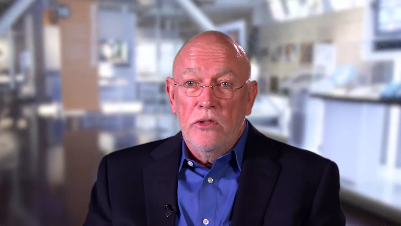
Computer History Museum
AI-assisted summary of Oral History of William David "Bill" Mensch Jr. — original source. Check the original for full context.
Source published:
Detailed notes
## Detailed walkthrough ### [00:06](https://www.youtube.com/watch?v=Ne1ApyqSvm0&t=6s) Growing Up in "Pleasant Poverty" in Rural Pennsylvania
Steve Diamond opens the interview at the Computer History Museum on November 10, 2014, introducing Bill Mensch for an oral history spanning his youth, his education, and his entry into the semiconductor industry. Bill begins by describing his upbringing on a dairy farm in Bucks County, Pennsylvania, roughly 35 miles north of Philadelphia. The farm was intensely rural and supported a herd of about 26 dairy cattle. Bill was the middle child among eight siblings, which naturally encouraged him to spend his time outside exploring rather than being cooped up inside the house.
The family lived in what Bill characterizes as "pleasant poverty," where survival and income depended entirely on the farm's small herd. The family had a radio and gathered eagerly around it to listen to *The Lone Ranger* as soon as the evening milking was finished, eventually acquiring a television when Bill was around ten years old. His father ran the farm as a small business passed down from Bill's grandfather. Bill later discovered that his father had harbored unfulfilled ambitions of attending Drexel University to become an electrical engineer. Looking back at his beginnings, Bill saw little early indication that he would one day make a career in high technology, remarking, “When you look at my past, I don't think there's many indications that I'd be sitting here talking to you.”
- Setting: Bucks County, Pennsylvania, approximately 35 miles north of Philadelphia. - Family dynamic: Middle child among eight children. - Farm operations: 26 head of dairy cattle providing the primary family income. - Paternal influence: His father operated the inherited family farm but had originally aspired to study electrical engineering at Drexel.
---
[02:40](https://www.youtube.com/watch?v=Ne1ApyqSvm0&t=160s) From Farm Laborer to College Student
Bill did not grow up harboring ambitions of becoming an engineer; instead, he expected to spend his life as a manual laborer. Life on a working farm revolved around concrete, demanding physical tasks: plowing fields, cutting and baling hay, hauling it to the barn, and milking cows every morning and evening. Because of this background, he loved physical work and the outdoors, never picturing himself working in an office environment.
When he took academic classes in high school, it was merely out of personal interest in math and science rather than a grand career design. He disliked subjects like English, history, and social studies because they lacked concrete certainty. In English, if an instructor asked what a poet meant, Bill felt the only logical person to ask was the poet. Math and science, by contrast, provided real, unambiguous answers. When his high school guidance counselor informed him at age eighteen that his coursework had prepared him for college, Bill was taken aback, as nobody in his family had ever attended college before. His initial exposure to electrical equipment came from his father, who kept electronics magazines around the house and had wired an industrial ship circuit breaker to a tractor-driven generator to keep the farm's milk coolers running during power outages.
---
[05:19](https://www.youtube.com/watch?v=Ne1ApyqSvm0&t=319s) Temple University and Early Employment at Polyphase
Bill enrolled in an engineering technology program at Temple University, focusing on applied equipment operation rather than foundational physics or theory. His initial motivation was straightforward: earn a credential, land a technician role, and make more money than he would as a common laborer. That assumption was quickly shattered once he entered the workforce. While working for construction contractor Henkels & McCoy, Bill had been pulling in about $150 a week with overtime, but his first technician jobs offered only around $85 a week. Realizing that an associate-level technology background would not provide the financial return he needed, Bill decided to pursue a full engineering degree, later explaining, “I decided to be an engineer to pay my mom back.”
After completing his studies and fulfilling military training obligations for the Army National Guard, Bill took his first post-college job in the spring of 1967 at Polyphase. Located in Bridgeport, Pennsylvania, across the Schuylkill River from Norristown, the company operated out of a grim, aging factory. Bill took the position on the recommendation of a friend who collected a $100 referral bonus for bringing him on board. Bill found the work and setting thoroughly depressing, leading him to quit after just three months without having another job lined up.
```mermaid flowchart LR accTitle: Bill Mensch Early Educational and Employment Path accDescr: Sequence diagram tracking Bill Mensch's transitions from farm life through early employment and education. A["Bucks County Farm<br/>(Agricultural Labor)"] --> B["Temple University<br/>(Engineering Technology)"] B --> C["Army National Guard<br/>(Military Training)"] C --> D["Polyphase<br/>(3-month tenure)"] D --> E["Philco-Ford<br/>(Semiconductor Lab)"] ```
---
[07:25](https://www.youtube.com/watch?v=Ne1ApyqSvm0&t=445s) Entry into Semiconductors at Philco-Ford and Moving West
Leaving Polyphase led Bill to Philco-Ford, an experience that marked his formal introduction to semiconductors. Ford had acquired Philco largely to secure automotive electronics, and the enterprise had also absorbed General Microelectronics (GMe), a pioneer in commercial MOS integrated circuits. At Philco-Ford, Bill encountered cutting-edge systems, such as a jet engine controller built using memory arrays and eight 1,024-bit ROM chips. Working as a technician, he analyzed the physical properties of solid-state devices: measuring transistor cutoff frequencies ($f_T$) and testing the thermal coefficients of voltage regulators mounted onto heat sinks.
Intrigued by semiconductor physics, Bill enrolled in night school at Villanova University, taking four engineering courses to prove to himself that he could handle a rigorous engineering curriculum. After doing well, he sought to transfer his roughly 109 credits from Temple toward a full bachelor's degree, hoping to finish within one or two years. When the local institution refused to accept his transfer credits, Bill decided to leave Pennsylvania for Arizona, inspired by a fraternity brother who had moved west. While his fraternity brother went to Arizona State University, Bill enrolled at the University of Arizona in Tucson.
- Philco-Ford exposure: Hands-on work with MOS technology stemming from the General Microelectronics acquisition, including 1,024-bit ROMs. - Technical duties: Measuring device physics, high-frequency cutoff parameters ($f_T$), and thermal transfer from semiconductor die packages to heat sinks. - Academic pivot: Completed four engineering courses at Villanova night school before moving to the University of Arizona after Temple credits failed to transfer.
---
[09:41](https://www.youtube.com/watch?v=Ne1ApyqSvm0&t=581s) Targeting Motorola and the Campus Interview
While working in Philco-Ford's television and consumer radio division, Bill observed that the engineering team spent considerable time reverse-engineering and evaluating Motorola's high-voltage circuit designs and breakdown voltages. Recognizing that companies only dissect the work of the market leaders rather than the followers, Bill resolved that Motorola was the benchmark in the industry and made it his definitive career objective upon graduation.
Bill finished his electrical engineering degree at the University of Arizona in two years. The program was rigorous, with professors actively writing the textbooks used in the curriculum, including early coursework in systems engineering. During his senior year, campus interview guidelines required spring graduates to sign up only during spring interview sessions. However, when the fall recruitment schedules were posted, Bill noticed that Motorola's interview sheet was completely empty because of their strict minimum requirement of a 3.3 grade point average. Possessing the required 3.3 GPA and unwilling to wait, Bill disregarded the schedule rules and signed his name on the empty sheet. Motorola's head of college recruiting, Jerry Fulton, arrived on campus and conducted the interview, starting an engaging conversation that paved the way for Bill's recruitment alongside Motorola manager Jack Hennison.
- Competitive insight: Observing Philco analyze Motorola's high-voltage TV circuits convinced Bill that “Motorola was the leader, so I wanted to work for a leader.” - Degree completion: Earned his engineering degree at the University of Arizona in two years. - Interview initiative: Took advantage of an empty fall interview slot reserved for students with a 3.3+ GPA despite being scheduled for spring graduation.
[12:15](https://www.youtube.com/watch?v=Ne1ApyqSvm0&t=735s) Landing the Motorola Job Despite a Rejection Letter
While wrapping up his engineering degree at the University of Arizona, Bill Mensch interviewed for post-graduation positions. He had an existing connection at Motorola: an executive who had previously worked at Philco-Ford two levels above Mensch's former boss. During on-campus recruitment, Mensch met with Motorola recruiter Jerry Fulton. Because Mensch already possessed two years of practical industry experience alongside his engineering technology background and degree, Fulton was eager to recruit him, telling him, “We got a job for you, partner.”
However, the formal spring campus interview did not go smoothly. Mensch walked out halfway through, assuming his earlier conversation with the hiring manager had already secured the role. When job offers arrived that spring, Mensch received offers from Martin Marietta in Denver and NCR in California for computer engineering roles. Confident in Motorola, he promptly declined both:
> “I promptly put it back in the mail, thanks but no thanks.”
When the long-awaited letter from Motorola finally arrived, signed by Fulton, it was an outright rejection stating they had no open positions. Panicked at having turned down his other options, Mensch remarked, “I want to jump in the mailbox to get back those other letters.” Instead, he telephoned Fulton immediately to clear up the confusion:
> “Jerry, you signed it.”
Fulton quickly brushed it off as an administrative blunder:
> “Oh Bill, there's a mistake, throw that away... That's a mistake, throw it away, there's another letter coming.”
With that phone call, Mensch secured his position at Motorola.
[14:31](https://www.youtube.com/watch?v=Ne1ApyqSvm0&t=871s) The Motorola Rotational Training Program and Early MOS Insights
At the time, Motorola ran a prestigious one-year training program consisting of four three-month rotations across different corporate divisions. Trainees were treated exceptionally well because the corporate training department covered their salaries, effectively granting host departments free engineering labor. Mensch used the opportunity to gain a comprehensive understanding of the entire company, intentionally tailoring his rotations across marketing, design, processing, and application engineering.
```mermaid flowchart LR accTitle: Bill Mensch Motorola Training Rotations accDescr: Four three-month rotations taken by Bill Mensch at Motorola spanning applications, circuit design, process development, and marketing.
subgraph Phase1["Rotation 1"] A["Applications & Marketing<br/>(MC6860 Modem Flowcharting)"] end subgraph Phase2["Rotation 2"] B["MOS Circuit Design<br/>(Modem Circuit Implementation)"] end subgraph Phase3["Rotation 3"] C["Process Engineering<br/>(MECL III Bipolar Modeling)"] end subgraph Phase4["Rotation 4"] D["Marketing & Economics<br/>(IBM Memory Yield Modeling)"] end
A --> B --> C --> D ```
- **Rotation 1: Applications Engineering (Marketing):** Mensch worked on the MC6860 low-speed 300-baud modem integrated circuit, collaborating with a consultant from modem manufacturer Anderson Jacobson. He created flowcharts and specified the circuit building blocks required to implement the modem architecture on silicon. - **Rotation 2: Circuit Design:** Moving directly into the design group, Mensch spent three months designing the actual circuits he had specified during his first rotation. - **Strategic pivot toward MOS:** Mensch recognized that metal-oxide-semiconductor (MOS) field-effect transistors (FETs) represented the future of integrated circuits. Bipolar technology, while the fastest at the time, was current-controlled and inherently slower when scaled, whereas FETs were voltage-controlled devices with superior performance scaling:
> “MOS was the future... The bipolar process was slower switching if you go to the highest performing circuits were going to be voltage control which is the FET.”
[17:00](https://www.youtube.com/watch?v=Ne1ApyqSvm0&t=1020s) Bipolar Process Modeling and Marketing Foreknowledge
Because a dedicated MOS process engineering slot was unavailable for his third rotation, Mensch joined the bipolar processing group handling MECL (Motorola Emitter-Coupled Logic), then the fastest switching logic family in the world. He worked on a triple-diffused process for MECL III, which involved diffusing the collector, base, and emitter directly into a bulk silicon background. Balancing junction depths was an exacting task; an improper emitter diffusion would punch through the thin base layer into the collector, creating a diode or a dead short.
To solve this, Mensch automated a process manual written by Motorola engineer Jim Dunkley: - He wrote a suite of five computer programs to simulate ion diffusion over variable times and temperatures. - The software modeled diffusion profiles to prevent emitter punch-through and accurately predicted breakdown voltages and junction characteristics.
For his fourth rotation, Mensch entered marketing to learn the business economics of semiconductors. Tasked with preparing a complex, multi-variable price quote for IBM, he modeled memory pricing over a seven-year learning curve spanning seven volume tiers and seven memory densities (producing a dense matrix across seven pages). Anticipating that administrative staff would struggle to type the massive table accurately, Mensch wrote a custom FORTRAN spreadsheet application to automate the pricing matrix: - He executed the program on a Texas Instruments Silent 700 terminal. - Because the Silent 700 printed on fragile, rolled thermal paper, he photocopied the generated output onto standard office paper to deliver a clean submission for IBM.
[19:42](https://www.youtube.com/watch?v=Ne1ApyqSvm0&t=1182s) A North Scottsdale Tornado and Entering the MOS Logic Group
By the end of his training program, Mensch had proven himself across diverse disciplines and collected five distinct full-time job offers from the departments he had rotated through, plus an offer from the high-voltage bipolar TV circuits group, which coveted his junction-breakdown modeling skills. Mensch originally planned to accept a permanent position in the bipolar processing organization and sent an inter-office memo to accept. However, he received no reply.
Meanwhile, Motorola's MOS marketing leadership intervened. Frustrated that the MOS logic design group was struggling to deliver functioning silicon, marketing pressured management to reassign Mensch:
> “We haven't really gotten circuits to work out of that MOS logic group, so we want you to work there.”
A week after Mensch reported to the MOS logic group, the manager of the bipolar department called him demanding to know his whereabouts. When Mensch explained that his memo had gone unanswered, the manager revealed an extraordinary excuse:
> “Bill, did you see the TV you know last week or the week before when that tornado sit down in north Scottsdale? Well, maybe he said that was my house. I was putting my house back together, that's why I didn't respond to you.”
Reflecting on the freak event that set his microprocessor trajectory in motion, Mensch observed, “A tornado changed my path.”
[22:19](https://www.youtube.com/watch?v=Ne1ApyqSvm0&t=1339s) Building the Standard Cell Logic Libraries
Once situated in the MOS logic division, Mensch took on a foundational project that other senior engineers actively avoided: characterizing and designing logic gate libraries. Motorola operated a custom logic initiative out of Boston (which Mensch jokingly referred to as "loco logic") that allowed computer companies to develop semi-custom ICs utilizing a standard cell library.
The job demanded painstaking characterization of drive strengths, input/output capacitances, propagation delays, and silicon parameters for every gate. Mensch methodically generated performance data sheets and design parameters across six distinct semiconductor process technologies: - PMOS metal-gate - PMOS silicon-gate - CMOS metal-gate - CMOS silicon-gate - NMOS metal-gate - NMOS silicon-gate
Mastering this broad array of fabrication recipes gave Mensch an unusually comprehensive grasp of semiconductor physics and circuit design across the entire portfolio:
> “I designed the local logic library for PMOS metal gate, PMOS silicon gate, CMOS metal gate, CMOS silicon gate, NMOS metal gate, and NMOS silicon gate. So I learned all the processes, so it was kind of like, wow, this is—now I know how it all works.”
This accomplishment quickly led to his next assignment: designing Motorola’s Process Control Monitor (PCM) test structures.
[23:44](https://www.youtube.com/watch?v=Ne1ApyqSvm0&t=1424s) Process Control Monitors and Transition to the PIA
Bill Mensch begins by describing his early work at Motorola on the NMOS enhancement-load process used for manufacturing memory chips and microprocessors. His responsibility was designing the process control monitor (PCM), test structures stepped into approximately five locations across each wafer. Technicians probed these test sites to confirm whether a manufactured wafer met process specifications. Following this assignment, Mensch was invited to join Motorola’s microprocessor design group. While a team of engineers was already dedicated to the central processor itself, the project urgently needed a dedicated engineer to create the peripheral interface adapter (PIA). Mensch was promptly reassigned to design this critical support chip.
The PIA functioned as the bridge between the digital core—the microprocessor and memory—and the external physical world. It allowed the system to drive solenoids, read external switches, and manage peripheral inputs such as keyboard scanning, where specific output pins pulsed matrix rows while input pins sensed key presses. Mensch viewed the assignment as a pivotal milestone in his career, noting, “so i got a wonderful introduction to the whole system by doing that peripheral interface adapter.”
```mermaid flowchart LR accTitle: PIA System Architecture accDescr: Diagram showing the PIA connecting the 6800 microprocessor core to external real-world peripherals. subgraph Core ["Motorola Processing Core"] MPU["6800 Microprocessor"] MEM["Memory Elements"] end subgraph Interface ["MC6820 PIA"] PIA["Peripheral Interface Adapter"] end subgraph Peripherals ["External Real-World Devices"] SW["External Switches & Keyboards"] ACT["Solenoids & Actuators"] end MPU <-->|"Data & Control"| PIA MEM <-->|"Memory Bus"| PIA PIA <-->|"Handshake & Port A/B"| SW PIA -->|"Drive Signals"| ACT ```
---
[25:08](https://www.youtube.com/watch?v=Ne1ApyqSvm0&t=1508s) Defining the PIA: Specifications, Die Sizing, and Layout Innovation
Mensch reflects on Motorola’s product definition pipeline, which was heavily steered by applications and marketing teams rather than IC designers. Marketing gathered requests from prospective customers and dictated features, resulting in a somewhat disorganized architecture for the flagship 6800 CPU. As Mensch puts it: “the 6800 microprocessor was thrown together by a lot of contributors so therefore the design group didn't really have much to say about what went into it.” He explains that sales representatives would frequently request one-off instructions, making the 6800 a somewhat arbitrary design loosely inspired by Digital Equipment Corporation's PDP-8, in contrast to the later 6502, which adopted the cleaner architectural philosophy of the PDP-11.
For the PIA, sales and management mandated a strict die footprint of 135 mils by 135 mils so the part could be manufactured profitably. The manufacturing process utilized 0.4-mil metal line widths with 0.4-mil spacing (a 0.8-mil pitch). To fit the required logic onto the prescribed silicon area, Mensch organized the floorplan so the microprocessor data bus interfaced on one side, driving a central data path across the die directly out to the I/O pads. This compact topology proved so innovative that Motorola patent attorney Charlie Hoffman filed for and secured what Mensch describes as the industry's first integrated circuit layout patent. Addressing the constitutional purpose of intellectual property, Mensch remarks: “you get a monopoly if you're willing to teach someone.”
When the assigned mask designer hit a wall and declared that a critical section of the layout could not be interconnected within the required space, Mensch took matters into his own hands. Possessing a deeper understanding of transistor and diffusion resistor geometry, he stayed up all night after a party on a Friday to hand-complete the layout himself, delivering the finished design on Monday morning ready for verification.
- **Mandated die dimensions:** 135 mils × 135 mils (in contrast to the larger 6800 CPU at 217 mils × 210 mils). - **Process geometry:** 0.4 mil line width and 0.4 mil spacing (0.8 mil metal pitch centers). - **Patenting achievement:** Received a landmark patent for the functional layout and placement topology of the IC.
---
[29:55](https://www.youtube.com/watch?v=Ne1ApyqSvm0&t=1795s) Rubylith, Early Simulation Tools, and Transistor Modeling
Integrated circuit layout verification in the early 1970s was an entirely manual, physical discipline without modern automated layout versus schematic (LVS) software. Layouts digitized on early Calma (Calma I) drafting systems drove flatbed plotters fitted with cutting knives to slice large-format sheets of Rubylith. Drafting technicians then hand-peeled the red film layer to create clear apertures where light could pass during photographic reduction. Mensch’s insistence on verifying designs through computer simulation sprang from advice he had received after his father passed away, when an IBM supervisor named George Rogers spoke to him at Temple University: “his one comment that i don't remember anything else i don't remember a hello or goodbye or anything get into computers.”
Taking that advice to heart, Mensch turned to Motorola engineer Frank Jenkins, who had arrived from Stanford or UC Berkeley and authored an analog circuit simulation program called TIME (transient integrated microelectronics circuit analysis), renamed M-TIME at Motorola. Mensch bridged the lab and software worlds by running parametric tests on his process control monitors and supplying real-world empirical data to Jenkins to refine the simulation deck. During these experiments, Mensch discovered a significant narrow-channel effect: narrow-width transistors exhibited higher threshold voltages than wider devices. This discovery had gone unnoticed by Motorola’s memory design group, which had to redesign several circuits after Mensch documented the phenomenon.
- **CAD/Verification methods:** Calma I layout terminals driving flatbed knife cutters on peelable Rubylith; complete absence of automated LVS checks. - **Circuit simulation tool:** M-TIME (Motorola TIME), an empirical transient circuit analysis engine developed by Frank Jenkins with fewer than 10 core device parameters. - **Device physics discovery:** Narrow MOS transistors exhibited unexpectedly higher threshold voltages, forcing revisions across Motorola's memory line.
---
[33:13](https://www.youtube.com/watch?v=Ne1ApyqSvm0&t=1993s) Chip Architecture, Bit-Programmable I/O, and Market Success
The final PIA design comprised roughly 1,000 to 1,500 transistors—a design so enduring that Mensch notes The Western Design Center still sells drop-in compatible replacements decades later. The chip featured 20 total I/O lines organized into two 8-bit bidirectional peripheral ports (16 lines) plus two dedicated hardware handshake lines per port (4 lines). Crucially, Mensch implemented a Data Direction Register (DDR) alongside the peripheral data register, permitting users to configure every single I/O pin independently as either an input or an output.
Competing peripheral parts of the era, notably from Intel’s 8080 family, forced entire 8-bit ports to be locked purely as all-input or all-output. The granular, bit-by-bit directionality of Mensch’s PIA made it vastly more flexible for real-world embedded control, leading customers to adopt it even when building around Intel processors. Mensch shares a humorous market dynamic involving NCR: “motorola would force them to buy a 6800 they were buying intel processors but buying my pa pias so intel marketing thought hey for every 10 pias you got to buy one microprocessor.” NCR purchased the mandatory 6800 CPUs just to get access to Mensch’s PIAs, often looking for places to offload the unwanted processors while pairing the Motorola PIA directly with the Intel 8080.
- **Gate complexity:** 1,000 to 1,500 MOS transistors. - **Port layout:** Two 8-bit bidirectional ports (16 data pins) alongside 4 dedicated handshaking control pins (2 per port). - **Key architectural differentiator:** Bit-level programmable Data Direction Registers (DDR), offering flexible mixed-pin configurations not available on Intel's peripheral chips.
[35:11](https://www.youtube.com/watch?v=Ne1ApyqSvm0&t=2111s) Architecture and Pinout of the Peripheral Interface Adapter (PIA)
Wrapping up the architectural overview of the Peripheral Interface Adapter (the Motorola 6820 PIA), Bill Mensch describes how the device coordinated data exchange with outside hardware. The peripheral interface side relied on a strict handshaking protocol: when an external peripheral grabbed the data present on the pins, it acknowledged the transaction by signaling back that the pins had been read. This mechanism supported both interrupt-driven and polled operation, allowing the host system to monitor exactly when data transfers concluded.
On the other side of the chip lay the interface to the microprocessor bus. This side featured eight bidirectional data pins, register addressing lines to select internal control and data registers, a read/write control line, a phase-two clock input, and connections for the power supply. Mensch notes that this entire complement of input, output, bus, and control lines was packaged into a standard dual-inline 40-pin package. As Bill Mensch sums it up regarding the complete interface: “that's basically a pia the other side of it is the interface to the microprocessor.”
- **Bus Interface:** 8 data pins, register addressing, read/write line, phase-two ($\Phi_2$) clock, power, and ground. - **Peripheral Interface:** Handshake control lines supporting polled and interrupt-driven transfers. - **Packaging:** Standard 40-pin DIP.
---
[35:44](https://www.youtube.com/watch?v=Ne1ApyqSvm0&t=2144s) Buffer Design, Clock Generators, and Circuit Physics at Motorola
Beyond the PIA, Mensch's circuit innovations were integrated across Motorola’s entire microprocessor chip family. Leveraging his earlier work developing standard cell libraries, he created the foundational input/output buffers and clock generators used by all the chips in the lineup. While others treated digital logic strictly as abstract gates, Mensch approached the silicon with an analog engineer's grounding in device physics. He calculated the exact capacitive and resistive loading along data paths and interconnect wiring, modeling those parasitics during simulation so transistors could be sized appropriately to achieve reliable switching speeds. As Bill Mensch points out: “and if you don't know what the capacitive loading is you don't know what transistor sizes will be required to switch in a certain time frame.”
That deep grasp of transistor-level physics remained a cornerstone of his later career. After founding Western Design Center, Mensch kept his fledgling business afloat by consulting for Xerox, where he taught their engineering staff how to design microprocessors from the ground up. Xerox's engineers struggled because they lacked this physical perspective on circuit assembly. Mensch demonstrated how transistor dimensions must directly account for wire and junction capacitance to meet target clock rates, bridging the divide between high-level logic and solid-state reality.
```mermaid flowchart LR accTitle: Transistor Sizing Workflow accDescr: Bill Mensch's methodology for sizing MOS transistors based on physical line parasitics. subgraph Analysis["Parasitic Analysis"] A["Interconnect / Data Path"] --> B["Calculate Capacitive & Resistive Load"] end subgraph Implementation["Circuit Synthesis"] B --> C["Model Load in Simulation"] C --> D["Size MOS Transistors for Target Delay"] end ```
---
[37:18](https://www.youtube.com/watch?v=Ne1ApyqSvm0&t=2238s) Chuck Peddle's Proposal to Leave Motorola for a New Microprocessor
While Mensch was in the middle of designing his next Motorola assignment—a programmable timer module (PTM)—Motorola began preparations to relocate its semiconductor operations from Phoenix, Arizona, to Austin, Texas. At that juncture, systems architect Chuck Peddle approached Mensch with an alternative. Peddle asked him bluntly if he really wanted to pack up his life and move out to Texas, and Mensch admitted he had no desire to go.
Peddle seized the opening to pitch an audacious venture: rather than moving to Austin to support a flagship processor they already viewed as flawed, they should assemble a core group of Motorola talent, find an independent company willing to sponsor them, and create an entirely new processor. Both engineers recognized that the Motorola 6800 was far too large and expensive to unlock high-volume cost-sensitive markets. Describing Peddle's pitch to break away, Bill Mensch recalls: “so chuck says hey how about if we we get a group together and we design the microprocessor we really want to do and you know that the 6800 isn't the right one it's too big.” Peddle took on the responsibility of scouting a landing spot while asking Mensch which essential engineers they needed to recruit out of Motorola to ensure the new design succeeded.
---
[38:17](https://www.youtube.com/watch?v=Ne1ApyqSvm0&t=2297s) Broken Promises: The First-Pass Bet and Engineering Bonus
Mensch’s departure was accelerated by two broken promises that left him thoroughly disillusioned with Motorola management. During a celebratory dinner at a local restaurant after the tape-out and release of the 6800 microprocessor and the 6820 PIA to manufacturing, Mensch got into an exchange over wine with MOS operations manager Otis Wolkins. Confident in his design discipline, Mensch offered a bold wager: he bet that his PIA would work completely on the very first silicon pass. Wolkins scoffed, stating that no complex integrated circuit had ever functioned on the first run. The two men agreed to a wager consisting of a high-end dinner for both engineers and their wives. When Mensch proposed the wharf in San Francisco, Wolkins countered with a luxury restaurant in Scottsdale featuring a $100 bottle of wine. Because automated Layout Versus Schematic (LVS) design verification software did not exist at the time, Mensch had personally checked the entire chip layout by hand five consecutive times. As Bill Mensch puts it: “you make a bet you better back it up.”
When the prototype silicon arrived from the fab, the PIA functioned on the first pass, but Wolkins reneged on the bet and never bought the dinner. Around the same time, Motorola was negotiating a second-source agreement with American Microsystems, Inc. (AMI). In a joint meeting, AMI management declared that if Mensch's PIA worked on the first pass, they would award him the project's first engineering bonus. That pledge sparked immediate friction with 6800 project leader John Buchanan, who felt that holding the overall engineering team together entitled him to the bonus instead. When the silicon worked and AMI never paid the promised bonus, Mensch realized his contributions were not being honored. Walking down the hallway at the 52nd Street facility, he ran into Jerry Foster, who asked if the rumors were true that he was quitting. Mensch confirmed his departure without hesitation, resolved to make his next venture a success. Reflecting on his mindset at that turning point, Bill Mensch explains: “no it was it was the fact that i needed to leave because not one but two promises were broken.”
- **The Dinner Bet:** A dinner including wives and a $100 bottle of wine in Scottsdale bet by Otis Wolkins against first-pass silicon success; Wolkins never paid. - **The AMI Bonus:** An engineering performance bonus promised by second-source partner AMI that was never delivered. - **Verification Method:** Manual five-fold visual and schematic check of the mask artwork in lieu of automated LVS verification tools.
---
[41:17](https://www.youtube.com/watch?v=Ne1ApyqSvm0&t=2477s) The Culture Clash at MOS Technology
Mensch, Peddle, and their cohort moved east to join MOS Technology in Norristown, Pennsylvania, entering an organization with a radically different corporate heritage. MOS Technology was staffed by former Texas Instruments personnel who ran a thriving business manufacturing p-channel MOS (PMOS) metal-gate chips for consumer calculators. The operations was spearheaded by a seasoned former TI manufacturing executive, while co-founder Don McLaughlin served as Vice President of Engineering, overseeing a logic team that designed sophisticated scientific and four-function calculator circuits.
When the Motorola expatriates walked through the door, the incumbent engineering staff was openly hostile to them. The calculator designers questioned why MOS Technology co-founder and president John Paivinen had recruited an outside team from the West Coast to build a microprocessor when they believed their internal team was fully capable of doing it themselves. Describing the resentment among the local staff, Bill Mensch remarks: “they're saying what how could john paven and the founding president how could he hire this group out of the west they don't know what they're doing and we know what we can do why why aren't we doing it.” Despite this cold reception, the new microprocessor project received the designation 6500—chosen informally because 65 was a lower number than Motorola’s 68—with the pin-compatible 6501 designated as their first production part, followed shortly by the iconic 6502.
---
[43:24](https://www.youtube.com/watch?v=Ne1ApyqSvm0&t=2604s) Assembling the Ex-Motorola Design Team
The defection from Motorola to MOS Technology involved a tightly organized team of eight people, supplemented by an additional local hire in Pennsylvania. Chuck Peddle served as the business mastermind and marketing visionary, negotiating the employment and product agreement with John Paivinen and defining the market opportunity. As Bill Mensch describes Peddle's central role: “he was the ring leader he was the he was the business guy he was the guy that said if we do this we can we can create a good business opportunity.” Terry Holt joined to oversee operations, while Bill Mensch and Rod Orgill headed up processor circuit design and architecture.
To translate the schematic architecture into silicon geometry, the team brought two experienced layout designers from Motorola, Harry Bawcom and Mike Janes, and hired a third layout specialist, Syd Hawkins, once they arrived in Pennsylvania. This eight-to-nine-person design and layout cell was featured in an *Electronic Engineering Times* (EE Times) photograph documenting the team responsible for creating the 6500 family. Operating under Peddle's commercial plan, this tight-knit group operated independently inside MOS Technology to bring the processor to market.
- **Business & Marketing Lead:** Chuck Peddle - **Processor Circuit & Logic Design:** Bill Mensch, Rod Orgill - **Operations Management:** Terry Holt - **Mask Layout Designers:** Harry Bawcom, Mike Janes, Syd Hawkins (hired locally)
---
[44:35](https://www.youtube.com/watch?v=Ne1ApyqSvm0&t=2675s) Bringing Up Depletion-Load NMOS and Dramatic Yield Improvements
MOS Technology did not possess an n-channel MOS (NMOS) manufacturing line when the Motorola team arrived, requiring them to build a new fabrication process from scratch. Mensch had previously advocated for an NMOS depletion-load process at Motorola, only to face stubborn bureaucratic resistance. During his time running Motorola’s Process Control Monitor (PCM) test vehicles, Mensch had leveraged crystal lattice physics—orienting structures to match silicon carrier mobility—and built depletion-load and enhancement-load test devices side-by-side on the same wafer. Producing depletion devices required just one extra ion-implantation mask step, yet it yielded faster switching speeds, reduced overall transistor count, and consumed less silicon area. When establishing the new MOS Technology line, Mensch and Peddle bypassed Motorola's reluctance and specified an NMOS depletion-load process using a streamlined flow of only seven to eight mask levels on roughly 3-inch wafers. As Bill Mensch recalls regarding Motorola's resistance to technical progress: “which going back to motorola days which was another reason why i left motorola is when you want to make a difference and somebody stands in your way for no apparent reason you kind of say what's going on here.”
The manufacturing results at MOS Technology completely outperformed Motorola's fab. At Motorola, NMOS process head Ed Armstrong had struggled with dismal wafer yields for months. In contrast, MOS Technology leveraged proximity printing rather than contact mask aligners (which degraded mask plates through physical contact) and utilized a proprietary mask-defect repair technique known as "spot knocking." By eliminating pinholes and particulate flaws on their photolithography plates, MOS Technology produced nearly defect-free masks. Consequently, while Motorola had celebrated single-digit yields, MOS Technology achieved an order-of-magnitude yield advantage on the 6502. Highlighting the stark contrast between the two operations, Bill Mensch observes: “he grew a long beard waiting for 10 good die per wafer and we were getting like 100 good die per wafer on the 6502 we had at least 10 times the yield per wafer.”
| Parameter | Motorola NMOS (6800 era) | MOS Technology NMOS (6502 era) | |:--- |:--- |:--- | | **Load Device Type** | Enhancement load | Depletion load (ion-implanted) | | **Mask Count** | Higher complexity | 7 to 8 masks | | **Lithography Masking** | Contact printing (mask wear) | Proximity printing / projection | | **Defect Mitigation** | Standard inspection | Proprietary "spot knocking" mask repair | | **Functional Yield** | Struggled to reach ~10 good dies/wafer | ~100 good dies/wafer (~10× yield improvement) |
[47:05](https://www.youtube.com/watch?v=Ne1ApyqSvm0&t=2825s) Mask Retouching and the On-Chip Clock Generator
Bill Mensch explains the significant manufacturing advantages MOS Technology held over Motorola. By employing a process called "spot knocking," they could compare two photomasks; since defects or pinholes would rarely occur in the exact same spot on both masks, technicians could manually apply a tiny bit of ink to cover holes and produce a near-perfect mask that could run hundreds of wafers without degradation. Because Motorola was not performing this kind of mask retouching, MOS Technology achieved drastically higher yields. This allowed them to sell the 6501 for $20 and the 6502 for $25 while still turning a healthy profit.
When the Motorola defector team arrived at MOS Technology to build a microprocessor, Chuck Peddle drove the high-level architecture while Mensch operated as the semiconductor engineer tasked with executing Peddle's vision. However, Mensch intervened when he recognized critical design bottlenecks in Motorola's competing 6800. Motorola charged $375 for the 6800 microprocessor and another $69 for an external clock generator—bringing the total system cost past $400 before adding any I/O chips. Worse still, producing the clock chip and the microprocessor on separate silicon wafers meant that process variations between wafers could pair a slow clock with a fast processor, triggering fatal race conditions.
While Peddle was away on a marketing trip, Mensch pitched Rod Orgill on integrating the clock generator directly onto the microprocessor die. By designing it in, an engineer would only need to attach a simple crystal and resistor (or an RC network) rather than an expensive external IC. When Peddle returned, Mensch assured him the on-chip clock was merely a metal-mask option that cost nothing in silicon real estate: the 6501 and 6502 shared the exact same base silicon, with the 6502 simply connecting the integrated clock generator at the metal layer.
```mermaid flowchart LR accTitle: Evolution from 6501 to 6502 Silicon accDescr: Diagram shows how shared base silicon with differing metal layers created the 6501 and 6502, leading to the settlement with Motorola. subgraph Die["Shared Silicon Die"] Base["Base Processor Layout"] Clock["Integrated Clock Generator"] end
Base -->|"Metal Option A<br/>(External Clock)"| M6501["MOS 6501<br/>• 6800 Pinout<br/>• $20 price"] Base & Clock -->|"Metal Option B<br/>(Internal Clock)"| M6502["MOS 6502<br/>• Unique Pinout<br/>• $25 price"]
M6501 -->|"Motorola Lawsuit<br/>Dropped in Settlement"| DeadEnd["Discontinued"] M6502 -->|"Surviving Product"| MassMarket["Market Standard"] ```
[50:01](https://www.youtube.com/watch?v=Ne1ApyqSvm0&t=3001s) The Bet with Rod Orgill and the Motorola Lawsuit
Because the 6501 preserved the pinout of the Motorola 6800, Orgill believed customers would prefer drop-in compatibility and predicted it would far outsell the 6502. Mensch disagreed, arguing that the convenience of an onboard clock generator made for a superior engineering solution. The two made a friendly wager while waiting for the first silicon to return from fabrication: > “I'm saying I think technology wins over marketing. Rod says marketing wins over technology.”
When Motorola filed a sweeping lawsuit against MOS Technology, the subsequent settlement forced MOS Technology to withdraw the pin-compatible 6501 entirely. With the 6501 removed from the market, the 6502 became the sole surviving product, and Mensch won his bet by default.
Mensch had never anticipated a lawsuit because he considered their design fundamentally different: MOS Technology used a brand-new depletion-load NMOS process rather than Motorola's enhancement-load process with complex bootstrap circuits, and the instruction set was completely original, meaning no 6800 opcodes could execute on their chips. In discovery, Motorola pursued patent infringement and trade-secret theft. The patent claim had technical merit regarding the 6520 peripheral interface adapter, which Mensch notes was identical to Motorola's 6820: > “Well, yeah, a 6520 chip is exactly the same as a 6820 chip; yeah, we violated your patent.”
The trade-secret allegations escalated when depositions revealed that one of the mask designers had brought Motorola schematics along during the move. Mensch insists these schematics were useless because the depletion-load process required entirely different circuit topologies, but the revelation nevertheless created severe legal friction. Ultimately, the trade-secret claims were dropped, and the dispute was resolved under a settlement centered on patent licensing and the discontinuation of the 6501.
[53:20](https://www.youtube.com/watch?v=Ne1ApyqSvm0&t=3200s) Decimal Arithmetic, the Atari Asteroids Bug, and Commodore's Takeover
The core patent granted for the 6502 covered its decimal correction hardware. Unlike the Motorola 6800, the 6502 allowed a programmer to set a single bit in the status register (the P register) to toggle between standard binary arithmetic and Binary Coded Decimal (BCD) math. Mensch wrote a complete Fortran simulation to verify every logic combination of the decimal-correct circuitry. All four key team members—Chuck Peddle, Bill Mensch, Rod Orgill, and Will Mathis—were named as co-inventors on the patent.
This BCD feature had tangible repercussions years later. Atari implemented it inside the coin-op arcade hit *Asteroids* to tally scores during the CRT display's vertical blanking interval. When Mensch subsequently designed the CMOS version of the 6502 (the 65C02), he had to implement decimal correction without infringing on his original patent, which added one clock cycle to the operation. That single extra cycle threw off Atari's video-synchronized timing loops and caused the asteroid graphics to tear apart on screen.
Despite the technical triumphs of the 6502, MOS Technology struggled financially. Because the microprocessor industry was still in its infancy, volume was low, and second sources like Synertek and Rockwell captured large contracts in California. Seeing an opening, Commodore founder Jack Tramiel capitalized on MOS Technology's vulnerability: > “MOS was going out of business; that's what Jack Tramiel saw—he saw blood in the water.”
Tramiel placed an enormous order for calculator chips representing six months to a year of MOS Technology's capacity. After the company expanded its headcount to roughly 200 workers to fulfill it, Tramiel abruptly canceled further chip orders. Deprived of calculator revenue before microprocessor sales could ramp up to Peddle's optimistic forecasts, MOS Technology was left defenseless, clearing the path for Tramiel to acquire the company outright. Mensch departed MOS Technology around March 1977.
[56:49](https://www.youtube.com/watch?v=Ne1ApyqSvm0&t=3409s) WESCON 1975: The Famous Mason Jar Debut
The team had officially transferred from Motorola to MOS Technology's payroll on August 19, 1974. Exactly one year later, by late summer 1975, they had brought up an entire semiconductor process, taped out the design, and prepared for commercial release. In September 1975, they unveiled the 6501 and 6502 in San Francisco during WESCON. Because show organizers barred them from selling silicon directly on the convention floor, Peddle set up shop in a room at the nearby St. Francis Hotel.
Peddle filled a large glass mason jar to the brim with working microprocessors, selling them to hobbyists and engineers for $20 and $25, while Mensch and Orgill mingled and drank beer with prospective buyers. The interviewer recalls attending the event as an enthusiast who could only afford the printed manuals rather than the processor itself. Meanwhile, back at the exhibition floor booth, crowds clamoring for data sheets overwhelmed the aisle: > “You could look down from the second floor and look down—here are all these people around our little booth knocking over a pinball—not a pinball, what do you call it, a pachinko machine or something like that with little balls—and our neighbors were not happy with us because they were getting trampled trying to get a data sheet.”
Attendees included Steve Wozniak, who purchased chips that would power the Apple I. When asked whether industry observers were skeptical that MOS Technology could deliver chips at under one-tenth the cost of the Motorola 6800, Mensch notes that as a bench designer he was insulated from market chatter. Chuck Peddle handled customer skepticism directly, occasionally courting doubt because of his tendency to massage details to fit his pitch.
- **August 19, 1974**: Team dropped from Motorola payroll and picked up by MOS Technology. - **August/September 1975**: 6501 ($20) and 6502 ($25) released; officially demonstrated at WESCON / St. Francis Hotel. - **March 1977**: Bill Mensch leaves MOS Technology following the Commodore acquisition.
[59:46](https://www.youtube.com/watch?v=Ne1ApyqSvm0&t=3586s) Demonstrating Competence and Designing the VIA Without a Computer
Mensch emphasizes that MOS Technology possessed deep semiconductor expertise that allowed them to dramatically undercut competitors' prices while still remaining profitable. Their manufacturing process yielded ten times as much on the same wafer sizes, and they were already accustomed to building larger chips for the calculator market at lower costs than their rivals. The operations were run by seasoned veterans from Texas Instruments, meaning the team had proven, high-level industry talent. Mensch was confident in showing schematics to anyone who doubted them: “We know what we're doing.” While Chuck Peddle handled marketing meetings, Mensch stayed immersed in hardware design.
During this period, Mensch designed the 6522 VIA (Versatile Interface Adapter) entirely by hand, without any computer-aided simulation tools. By that point in his career, he had mastered transistor sizing by intuition and experience. Proving to himself that he could produce a fully functional, complex chip without needing an expensive mainframe simulator was a pivotal milestone that gave him the confidence to know he could eventually launch his own independent company.
[01:00:58](https://www.youtube.com/watch?v=Ne1ApyqSvm0&t=3658s) Designing the VIA on an Arby's Napkin and the Macintosh Mouse Port
The functional definition of the 6522 VIA was born during a lunch meeting between Mensch, Chuck Peddle, and application engineer Will Mathis at an Arby's restaurant in Norristown, Pennsylvania. Peddle had returned from discussions noting that customers urgently needed an onboard timer and a serial port integrated with peripheral I/O. Sketching out the architecture on a paper napkin, Mensch calculated the register constraints: combining a PIA, a timer, and a serial port expanded the register count, requiring it to be constrained to 16 addressable registers.
```mermaid flowchart LR accTitle: Evolution of 6522 VIA Feature Set accDescr: Diagram tracing the napkin requirements through two layout revisions to its eventual deployment in the original Macintosh.
subgraph Ideation ["Arby's Lunch Meeting"] A["6820/6520 PIA Core"] --> D["6522 VIA Concept"] B["Hardware Timer"] --> D C["Serial Port"] --> D end
subgraph Silicon ["Design & Iteration"] D --> E["16 Addressable Registers"] E --> F["First Pinout Layout"] F --> G["Redesign for Compatibility"] end
subgraph Legacy ["Field Application"] G --> H["Synchronous 8-bit Port"] H --> I["Apple Macintosh Mouse Interface"] end ```
After completing the initial silicon layout, Peddle requested changes for system compatibility, forcing Mensch to redesign the entire chip a second time with a different pinout. When Mensch originally asked Peddle what type of serial port was required, Peddle simply responded, “just any serial port.” Consequently, Mensch implemented an unusual 8-bit synchronous shift register rather than a full asynchronous UART. Though unconventional, this unique serial port found notable real-world use, including serving as the mouse interface on the original Apple Macintosh. Looking back, Mensch reflects: “If I had to do all over again, I said, 'Chuck, we need a UART plus a timer plus the I/O pins, and we got a really good product.'”
- **Register Budget**: Kept to exactly 16 registers to fit system addressing schemes. - **Port Architecture**: 8 bits in, 8 bits out, operating synchronously rather than asynchronously. - **Apple Adoption**: Utilized in the original Macintosh hardware to interface with the mouse.
[01:02:48](https://www.youtube.com/watch?v=Ne1ApyqSvm0&t=3768s) Division of Labor, System Software, and Commodore Video Chips
Mensch maintained strict boundaries between his responsibilities and those of his colleagues. Chuck Peddle oversaw marketing and authored the software manual, while Will Mathis handled customer applications and wrote the hardware manual, leaving Mensch free to focus entirely on silicon design. While Mensch assisted with manufacturing logistics for early gaming chips—such as Atari's *Pong* silicon fabricated at MOS Technology—he stayed out of broader board-level architectural debates.
When Commodore later developed the PET, VIC-20, and Commodore 64, internal philosophies diverged. Peddle championed the Commodore PET as a serious, professional machine equipped with an IEEE-488 bus, which Mensch describes: “He was PET—that's industrial-strength stuff... this is real engineering, this is a real computer.” However, the PET suffered commercially from Jack Tramiel's decision to include a cheap chiclet keyboard. In contrast, the consumer-oriented VIC-20 and Commodore 64 moved toward entertainment, driven by design engineers like Al Charpentier, who created custom sprite hardware for video games.
[01:05:13](https://www.youtube.com/watch?v=Ne1ApyqSvm0&t=3913s) Driving Composite Video and the 6502’s Competitive Advantage
To demonstrate the capability of his design, Mensch pulled off an engineering feat that Peddle believed was impossible: in just two weeks, he harnessed the VIA's serial port to directly generate a composite video signal on a standard television set, creating a playable barnstorming flight game. Tramiel had told him it could not be done, but Mensch determined the precise timing by clocking the processor at 4 MHz.
At that speed, the 6502 was running two to four times faster than competing chips from Intel or Motorola. Mensch attributes this performance to the depletion-load NMOS process, which delivered superior clock rates at lower power consumption. Combined with aggressive pricing and an intuitive instruction set, the 6502 held an unbeatable market position. Mensch summarizes the total architectural edge: “So we were easier to use, lower power, lower cost, and twice as fast—you got a winner. Any one of those things, you got a winner. All four of them: slam dunk.”
| Feature Metric | MOS Technology 6502 | Contemporary Rivals (Intel / Motorola) | |:--- |:--- |:--- | | **Clock Speed** | Up to 4 MHz (2× to 4× faster) | Typically 1 MHz to 2 MHz | | **Unit Price** | ~$20-$25 (roughly 1/10th cost) | ~$179-$300 | | **Power Consumption** | Significantly lower | Higher power draw | | **Process Tech** | Depletion-load NMOS | Standard enhancement-load NMOS | | **Ease of Use** | Streamlined instruction set & pipelining | Complex register architectures |
[01:06:31](https://www.youtube.com/watch?v=Ne1ApyqSvm0&t=3991s) Market Adoption Realities and Clock Oscillator Expertise
Despite the 6502’s technical superiority, Mensch understood that raw architecture alone does not decide industry standards. Major firms like DEC initially favored established giants like Motorola or Intel because of corporate marketing muscle, reliable supply guarantees, and business relationships, which MOS Technology struggled to navigate. Mensch remarks on these commercial dynamics: “It's not about whether the architecture is better, it's: do you know what you're doing in manufacturing? Will you support your customers' need?”
Addressing technical questions about the 6502's integrated on-chip clock generator, Mensch notes that it worked on the very first silicon pass without requiring revisions, thanks to his analog background as Motorola’s former clock specialist. His reputation as an oscillator expert was so established that while consulting at ICE (Integrated Circuit Engineering), he was brought in to redesign an unreliable 10 kHz Statek crystal oscillator for an implantable cardiac pacemaker. He successfully re-engineered the circuit to run with a 32 kHz crystal. The design was put straight into production to remedy pacemaker recalls; the customer simply called him on a Saturday morning to confirm it worked perfectly, and Mensch never even laid eyes on the physical chip. Decades later, his collaborator David Gray helped refine those oscillator designs even further for Western Design Center’s W65C134 and W65C265 microcontrollers.
[01:09:45](https://www.youtube.com/watch?v=Ne1ApyqSvm0&t=4185s) Motivation to Depart MOS and the Ricoh Super Nintendo Contract
Mensch’s drive to build standard microprocessors for industrial, commercial, and gaming applications eventually spurred him to strike out on his own. He avoided building finished consumer gadgets like calculators himself, preferring to provide core silicon engines for the broader electronics industry.
That trajectory culminated in a landmark deal with Japanese semiconductor manufacturer Ricoh. Mensch granted Ricoh an exclusive manufacturing license to supply 65816-based 16-bit processor cores to Nintendo for the Super Famicom (Super Nintendo Entertainment System). Mensch recalls with amusement how his son became an immediate celebrity in their neighborhood when he received an early Japanese Super Famicom directly from Ricoh, completely equipped with Japanese text and characters before the console had even launched in the United States.
- **Nintendo Processor Core**: The 16-bit W65C816S architecture, licensed through Ricoh. - **Contractual Scope**: The only exclusive licensing agreement Mensch ever granted to a partner company.
[01:10:51](https://www.youtube.com/watch?v=Ne1ApyqSvm0&t=4251s) Leaving MOS Technology and Rejecting Xerox
As the business climate deteriorated around 1977, MOS Technology was in dire financial straits and looked like it was going to go out of business. During this period, Chuck Peddle shifted away from being the microprocessor team leader toward becoming a systems-level person, aligning himself with California operations as Commodore was acquiring MOS Technology in what Bill Mensch describes as a depressed situation or fire sale. Mensch decided to leave during or shortly after the Commodore acquisition around the time the Apple II was being introduced. He had no desire to cater to low-end consumer toys, explaining his engineering philosophy: “I only want to design something that goes into high-volume production used by many and so looking at feeding the game or calculator consumer products that wasn't my cup of tea that's not what I wanted to do.”
Exploring his career options while still employed at MOS Technology, Mensch flew to El Segundo, California, to interview at Xerox with Bob Markle (or a similar name). Xerox was eager to hire him and offered to double his salary because experienced microprocessor designers were exceedingly scarce. However, when Mensch inquired about the actual job responsibilities, he learned he would be in a pure research laboratory where designs were handed off to production teams who would completely redesign them for manufacturing. Mensch balked at the wastefulness of that model, telling his interviewer, “Bob, I'm in the wrong place. My designs don't get redesigned, they go into volume production right away, or why didn't I do it right in the first place?” He made it clear he was not a research academic: “I'm not a research guy, I'm somebody that wants to make things happen, and how I know I'm making them happen because they go into volume production, they're used by people, we don't throw away designs, we just do it the right the first time.” Politely declining the doubled salary, he returned to Pennsylvania to figure out his next move.
[01:14:04](https://www.youtube.com/watch?v=Ne1ApyqSvm0&t=4444s) Integrated Circuit Engineering (ICE) and the Seminar Circuit
Mensch found his next opportunity with Glen Madland at ICE (Integrated Circuit Engineering) in Arizona. Madland had been the first design manager at Motorola in Phoenix and had recognized early on that the industry needed someone to teach the market how to use integrated circuits, which operated on completely different principles than discrete resistors and transistors. Seeing the value of having a proven microprocessor designer on staff to educate industry leaders, Madland hired Mensch to teach global seminars, including a dedicated course titled "Microprocessors for Management." Mensch accepted the job at a lateral salary—receiving no raise—because returning to Arizona felt right for his family, which now included two children under four years old.
The transition from hands-on circuit design to public lecturing proved intensely jarring. Addressing rooms of 50 paying executives and engineers, Mensch developed severe, incapacitating migraine headaches within the first hour of sessions, yet had to push through without any backup speaker. He struggled with audience reception: while peers like Howard received stellar reviews, Mensch initially received failing marks from attendees. When he vented his frustration to Madland, his boss offered a startling reality check: “Bill, you haven't figured it out yet, we're in the entertainment business.” Madland explained that attendees traveled from freezing climates to warm Arizona expecting an enjoyable experience, whereas Mensch was overwhelming them with dense technical detail they could not digest. Reluctantly, Mensch dumbed down his technical material, and while his evaluation scores immediately rose, the compromise felt hollow and unfulfilling: “This doesn't feel right at all, so I can't do this.”
```mermaid flowchart TD accTitle: The Glen Madland Dilemma at ICE accDescr: Flowchart illustrating Bill Mensch's dilemma while teaching at Integrated Circuit Engineering (ICE). subgraph ICE["ICE Seminars: High-Density vs Entertainment"] A["Deep Technical Detail"] --> B["Attendees Overwhelmed & Headache"] B --> C["Failing Student Evaluations"] D["Dumbed-Down Material"] --> E["Entertained Audience"] E --> F["High Grades (Felt Inauthentic to Mensch)"] end subgraph Epiphany["Glen Madland's Life Formula"] G["Doing what you want to do"] H["Living where you want to live"] I["Being comfortable financially"] end C -.-> G F -.-> G ```
[01:18:24](https://www.youtube.com/watch?v=Ne1ApyqSvm0&t=4704s) The "What's It All About?" Epiphany and Reverse Engineering
Standing at the coffee bar outside their adjoining offices, Mensch asked Madland a foundational question: “What's it all about?” Madland gave an answer that stayed with Mensch forever: “For me, it's about doing what you want to do, living where you want to live, and you're comfortable.” Returning to his desk, Mensch took inventory of his own life: he loved living in Arizona, but his second child had just been born on a credit card because ICE lacked maternity benefits, leaving him deeply uncomfortable financially. Crucially, he was not doing what he wanted to do. Comparing himself to baseball pitcher Denny McLain, who had an unprecedented 30-win season, Mensch felt as though he had just pitched a world-class no-hitter with the 6502 only to find himself sitting on the sidelines of his own industry: “I just pitched a no-hitter, wins 30 games, and I'm out of the business; I need to get back in the business.”
While at ICE, Mensch worked on extensive reverse-engineering projects for commercial clients, charging a fixed fee of $5,000 per processor. To handle the workload, he organized a mini assembly line, employing a bipolar consultant to assist with bipolar components while he traced the internal registers, logic, and transistors. Notable highlights of this period include: - Reverse-engineering competing dynamic RAM chips for Shell Oil Company, which owned early DRAM patents and was pursuing Mostek. Mensch examined the Mostek circuits designed by Bob Proebsting (a former Shell designer) and demonstrated the use of balanced bit-line architectures and sense amplifiers. - Training engineers at NCR on microprocessor design, working around their proprietary bipolar technologies such as integrated injection logic ($I^2L$) or emitter-coupled logic (ECL)—a task he completed faithfully despite believing bipolar was the wrong direction for microprocessors. - Receiving an overture about a year into his time at ICE from Commodore's Jack Tramiel, who sought low-power CMOS calculator chips. Tramiel was utilizing a Southern California semiconductor firm (believed to be Frontier Semiconductor) for CMOS manufacturing. This demand directly paved the way for Mensch to step away from consulting and establish the Western Design Center (WDC).
[01:22:32](https://www.youtube.com/watch?v=Ne1ApyqSvm0&t=4952s) Setting Up ICE Simulation and the Risk Dispute with Glenn
Bill Mensch wanted to establish a full integrated circuit design capability at Integrated Circuit Engineering (ICE). To achieve this, he needed both circuit and logic simulation tools. He tracked down a circuit simulator and a logic simulator originating from Bowmar (the calculator firm, where ICE had earlier ties). Frank Jenkins, an engineer Mensch knew from their days at Motorola, had developed both tools. Jenkins had left Motorola and was actively selling these simulators prior to the advent of tools like Verilog. Mensch got the software running on an accounting firm's Prime 300 minicomputer, which utilized virtual memory and could handle virtually any size logic circuit.
```mermaid flowchart TD accTitle: The Roadblock to In-House IC Design at ICE accDescr: Diagram showing how Mensch set up simulation tools at ICE, only to be blocked by Glenn's risk aversion and mutual mistrust between Glenn and Jack Tramiel.
subgraph Infrastructure["ICE Tool Infrastructure"] A["Frank Jenkins<br/>(ex-Motorola)"] -->|"Simulators"| B["Prime 300<br/>Virtual Memory Minicomputer"] B --> C["Mensch establishes IC design base"] end
subgraph Stalemate["The Commercial Impasse"] C --> D{"Glenn's Stance"} D -->|"Rejects IC design"| E["'Chips don't always work'<br/>Too much risk to goodwill"] F["Chuck Peddle calls:<br/>Tramiel wants calculator chips"] --> G{"Negotiation Attempt"} G -->|"Glenn"| H["'Jack ripped me off,<br/>never working with him'"] G -->|"Tramiel"| I["'Glenn ripped me off,<br/>won't deal with ICE'"] end
E --> J["Mensch leaves to start own company"] H --> J I --> J ```
Mensch planned to market logic and circuit simulation services through ICE while building an in-house design foundation. However, Glenn Madland pushed back against actual chip design due to commercial liability:
> “Glenn says, ‘You know, there's a problem with designing integrated circuits: they don't always work.’”
Mensch countered that chips do work if you know what you are doing, but Glenn remained unyielding:
> “‘Yeah, but there's a risk involved there, and you can risk our good, good will—our relationship we have, so I can't really take that risk.’”
As Mensch wondered how he would continue designing chips, Chuck Peddle unexpectedly reached out with an opportunity: Jack Tramiel needed calculator chips designed for Commodore. When Mensch pitched the opportunity to Glenn, Glenn flatly rejected it:
> “Glenn says, ‘No, Jack ripped me off, Jack owes me money, it's not good, I never want to do anything with Jack ever again.’”
Mensch then asked Chuck if Commodore would hire ICE to do the design work with the simulators and tools he had configured, but Peddle delivered the exact mirror image of the complaint:
> “‘Nope, Jack doesn't want to have anything to do with Glenn.’”
Astonished that each man accused the other of ripping him off, Mensch realized he could not pursue chip design inside ICE and resolved to establish his own independent company.
---
[01:25:34](https://www.youtube.com/watch?v=Ne1ApyqSvm0&t=5134s) The Las Vegas Casino Meeting and Deal Structure
On Mother's Day weekend in May 1978 (around May 13), Mensch traveled to Las Vegas to meet Jack Tramiel and Chuck Peddle at a casino. When Mensch arrived, Tramiel was down $10,000 at the tables, but his fortunes abruptly reversed and he won $17,000. Crediting Mensch with bringing him good luck, Tramiel invited them up to his hotel suite to talk business. Tramiel sat opposite, Chuck sat alongside, and Mensch sat on the sofa. Tramiel opened by asking Mensch what he wanted to do, and when Mensch stated he wanted to design ICs for Commodore, Tramiel immediately made an aggressive executive pitch:
> “‘I'll give you a department within Commodore, I'll make you vice president of Commodore—a whole division. I'll pay you more than I pay Chuck.’”
This sudden offer left Chuck Peddle visibly unsettled. Mensch declined the corporate role, telling Tramiel he insisted on having his own independent firm. Leveraging his experience drafting client agreements at ICE, Mensch proposed a milestone-driven contract where Commodore would cover his direct costs so he would break even, with all profits tied to unit royalties:
> “‘I get a royalty off of each chip, so I don't make anything if it doesn't go into volume production. I believe in what I do. I believe what I do will be—produce volumes; that's where I'll make the profit, I'll break even, and that's how it works.’”
- Tramiel offered a full division, a vice presidency, and higher pay than Chuck Peddle to keep Mensch in-house. - Mensch structured the agreement so upfront milestone payments merely covered overhead and design costs. - The upside was based strictly on a royalty per unit sold, ensuring Mensch had a direct stake in volume production.
---
[01:27:40](https://www.youtube.com/watch?v=Ne1ApyqSvm0&t=5260s) Royalty Terms, Accounting Pitfalls, and Working with Chuck Peddle
Mensch’s insistence on a gross unit royalty stemmed directly from the bitter lessons learned during his departure from MOS Technology. The compensation package Chuck Peddle had previously negotiated there rewarded the team with a percentage of *net profits*:
> “Chuck put together the deal—guess what it is: a percentage of profits. Well, you get to looking at who's cooking what books, you know, when will there ever be profits here? Well, you know, it's how you do your accounting, what are you assigned to this and any other thing, so there were some really unhappy folks.”
Determined never to repeat that mistake, Mensch negotiated a royalty tied directly to unit volume and sales price rather than profitability:
> “‘I don't care if you make a profit or not, that's your problem, but I'm getting a percentage of whatever you sell it for.’”
Mensch reflects warmly on his enduring friendship with Chuck Peddle despite past frictions, describing their dynamic as a synergy between two distinct temperaments. Comparing Peddle to Steve Jobs, Mensch explains that Peddle possessed a rare ability to orchestrate complex deals:
> “‘There's got to be a pony around here with all this crap,’ and so I think Chuck can put together some interesting deals that only Chuck can put together, it's just like a Steve Jobs in a way, and so if you know him that way, life is exciting, so to speak—opportunities.”
---
[01:29:40](https://www.youtube.com/watch?v=Ne1ApyqSvm0&t=5380s) Reverse-Engineering Toshiba and Tramiel’s Tactical Gambit
Although Mensch successfully engineered the chips, Commodore never put his designs into production. Tramiel's objective was commercial leverage rather than manufacturing. Mensch reverse-engineered the Toshiba LC5003 (LC5K3), a complex serial-processor calculator chip. Reverse-engineering this chip proved exceptionally demanding because Toshiba had embedded hidden ion-implanted resistors under the surface that could not be seen under optical inspection:
> “It's hard to reverse engineer an LCD—implanted resistors, you can't see them on the surface, so you go, ‘How is that happening?’ And you have these nodes that aren't connected up to anything; well, they've implanted resistors in there you couldn't see, so I had to figure that out.”
In addition to buried resistors, Toshiba had placed deliberate "phantom circuits" across the die that performed no electrical function and served purely to mislead competitive teardowns. Mensch deciphered the architecture and delivered a fully functioning equivalent, but Tramiel used the completed design solely to force Toshiba to cut its prices:
> “What he did was, when I—I duplicated the LC5K3 chip out of Toshiba... but guess what Jack wanted to do: he wanted to get the Japanese price, which was half of the American price, so he wasn't going to buy any chips—he wasn't going to build any of my chips. He wanted the chip to design so he could go back as a negotiating [tool].”
Mensch noted that as a natural gambler, Tramiel cared strictly about bottom-line component costs rather than running an internal silicon fabrication line if Toshiba could be pressured into matching target pricing.
- The target chip was the Toshiba LC5003 (LC5K3) serial-processor calculator IC. - Toshiba employed optical decoys, including dummy "phantom circuits" and buried ion-implanted resistors beneath unconnected metal nodes. - Tramiel leveraged Mensch’s working design to secure the Japanese domestic component price (roughly 50% of the export price charged to American firms).
---
[01:31:31](https://www.youtube.com/watch?v=Ne1ApyqSvm0&t=5491s) Architecting a Variable-Nibble 4-Bit RISC Scientific Processor
After the serial five-function calculator project, Commodore aimed to enter the scientific calculator market. Serial calculation was far too slow for scientific operations, prompting Mensch to architect a parallel 4-bit RISC processor. The standard 8-bit NMOS 6502 core was unsuitable because scientific operations require variable-precision floating-point arithmetic (ranging from 24-bit single-precision mantissas and exponents up to 64-bit double precision) while keeping the silicon die size tiny:
> “A 4-bit RISC processor—it had like 16 instructions, but what I had was a field, a 4-bit field that would tell you how many nibbles. So if I wanted to do a 64-bit, I'd have a 16 4-bit nibbles... that could do 4, 8, 12, 16, all the way to 64-bit.”
Mensch developed this architecture alongside a software programmer named Shiraz (who worked either from India or Northern California), with Chuck Peddle largely absent from day-to-day technical development. Mensch also sought help from Will Mathis. Although primarily a semiconductor device engineer who had to absorb microprocessor architectural theory from market demands, Mensch engineered the 4-bit RISC instruction set to directly interface with liquid crystal displays (LCDs) while efficiently executing arbitrary multi-nibble mathematical operations without the die-area overhead of an 8-bit core.
- **Architecture:** 4-bit parallel RISC processor with a compact ~16-instruction set. - **Variable-Length Math:** A dedicated 4-bit field specified the nibble count, supporting arithmetic word lengths from 4 bits to 64 bits in 4-bit increments (4, 8, 12, 16... 64 bits). - **Target Workloads:** Fast scientific floating-point math (e.g., 24-bit mantissa/exponent representations and 64-bit precision) and direct driving of LCD display interfaces. - **Personnel:** Designed by Bill Mensch in collaboration with firmware engineer Shiraz, with consultation from Will Mathis.
[01:34:14](https://www.youtube.com/watch?v=Ne1ApyqSvm0&t=5654s) The DRAM Achilles' Heel in Calculator Design
Mensch reflects on an early design flaw that proved fatal for a low-power calculator chip project. Jack Tramiel’s son, Sam Tramiel, was in Japan at the time and understood the rigorous demands of the handheld calculator market: even a single microampere of standby current was intolerable. Unaware of this strict power constraint, Mensch drew upon semiconductor techniques he had studied during his stint at Integrated Circuit Engineering (ICE) under Glen Madland. Attempting to save silicon area compared to bulky static memory cells, he integrated a single-transistor, non-self-aligned metal-gate dynamic RAM (DRAM) onto the chip.
Although the DRAM functioned as designed, its reliance on periodic refresh cycles pushed standby power dissipation far beyond the 1 µA ceiling. Mensch candidly acknowledges this design choice as an Achilles' heel born of engineering isolation: “So here I am thinking the semiconductor technology that I knew, and I got it to work and it works fine—worked fine, but too much power.” The refresh requirement meant the part consumed well over a microamp, rendering it unsuitable for the Japanese calculator market.
- Sam Tramiel was tracking Japanese calculator industry specifications, where standby current had to remain strictly below 1 µA. - Mensch implemented a 1-transistor (1T) metal-gate DRAM using non-self-aligned gates to minimize die area. - The continuous refresh cycle inevitably drew excess current, spoiling the chip’s viability for battery-operated handheld devices.
---
[01:35:24](https://www.youtube.com/watch?v=Ne1ApyqSvm0&t=5724s) Commodore’s Exit, Jack Tramiel’s Exclusivity, and the Xerox Lifeline
When asked how the Western Design Center (WDC) became involved with the 65C02, Mensch explains that Commodore had zero interest in a CMOS version of the 6502. The existing NMOS 6502 was already far lower in power than competing microprocessors from Intel or Motorola, providing plenty of efficiency for personal computers like the Commodore PET.
Around late 1980, after internal strife led Irving Gould to oust Jack Tramiel from Commodore—a development Mensch only fully understood years later upon reading Brian Bagnall's book *On the Edge*—Commodore abruptly cut ties with Mensch’s fledgling operation. A design manager from California arrived with a truck and stripped the office of every piece of equipment they claimed to own. Jack Tramiel had imposed strict exclusivity terms on Mensch: “Jack said exclusive: ‘You don't work for anybody else, you work for me, you don't work for anybody else.’” Because Mensch had interpreted this restriction literally, he had deliberately avoided building a sales pipeline or pitching other clients. Suddenly, he was left with an empty office, a $50,000 promissory note due in six months, three children under the age of six, and zero paying customers.
In desperation, Mensch called Bob Marco at Xerox. Xerox had earlier attempted to secure a portion of Mensch's consulting time by offering Commodore access to their most advanced fabrication process, but Commodore vice president Bud Frye had flatly refused, insisting on 100% of Mensch’s dedication. Now unencumbered, Mensch flew out on a credit card to meet Marco just before the Christmas holidays. After hearing that Commodore had vanished, Marco summoned his secretary, who returned with an envelope containing a $25,000 check. Stunned, Mensch asked why Marco would hand over that kind of money without a contract. As Mensch recounts, Marco offered a blunt reality check about rare engineering talent: “Bill, when a microprocessor design engineer becomes available, you lock them down.” Xerox engaged Mensch to teach their internal engineering team how to design microprocessors. To deliver on the agreement, Mensch hired his sister Diane and trained her in mask design in just five weeks.
```mermaid flowchart LR accTitle: Western Design Center Transition from Commodore to Xerox accDescr: Diagram tracing the fallout from Commodore's departure to Xerox's emergency funding. subgraph Commodore["Commodore Departure (Late 1980)"] A["Jack Tramiel ousted by Irving Gould"] --> B["Commodore truck repossesses equipment"] B --> C["Mensch left with $50k note & 3 young kids"] end subgraph Xerox["Xerox Intervention"] C --> D["Call to Bob Marco at Xerox"] D --> E["Marco provides immediate $25k retainer"] E --> F["Contract to train Xerox engineers"] F --> G["Mensch trains sister Diane in mask design"] end ```
---
[01:40:32](https://www.youtube.com/watch?v=Ne1ApyqSvm0&t=6032s) Mitel, GTE, and the Genesis of OxyCMOS
The path to the CMOS 65C02 emerged out of professional ties Mensch had formed while teaching microprocessor seminars for management at ICE. Attendees included Fran Krch, a marketing executive from Micro-Mo Electronics / EM Semi, and Dr. Desmond Sheehan, an executive with a doctorate from Stanford and an undergraduate degree from Scotland. Sheehan, then Vice President of Technology at GTE Lenkurt, had convinced GTE corporate to invest heavily in semiconductor manufacturing and urgently needed silicon designs to justify the capital expense of their fabrication line.
Sheehan dispatched Mensch on his first international flight to GTE’s ATEA division near Antwerp, Belgium, to analyze a telephone key-system design based on the Motorola 6802. Around that time, Mensch discovered that Mitel Semiconductor possessed a cutting-edge unipolar-doped polysilicon, oxide-isolated CMOS process that dramatically reduced parasitic capacitance. Recognizing that this process was the future of low-power computing, Mensch established his own proprietary set of design rules dubbed "OxyCMOS" (Oxide-Isolated CMOS).
Through serendipity, Mensch learned that Mitel had licensed its oxide-isolated CMOS process and a 6802 implementation to GTE. He contacted Mitel's sales arm and flew on short notice to meet them in freezing winter weather (roughly -30°F) in Canada via an airport connecting to Ottawa. Mitel revealed that their contract design team in Lake Tahoe had botched their CMOS 6802 design: it crawled at an abysmal 250 kHz rather than its 5 MHz target frequency. The designers had neglected the project in favor of skiing and partying (“two forms of snow,” as Mensch dryly remarks), and Mitel had promptly fired them. Mensch evaluated the design and told Mitel that while hitting 5 MHz was unrealistic without a total ground-up redesign, he could salvage the layout to run reliably at 1 to 2 MHz—matching the performance of the NMOS original. Mitel wrote him an upfront check for $15,000 on the spot, providing another vital financial runway.
Equipped with the functional requirements gathered from GTE's ATEA division in Belgium, Mensch drafted two distinct development proposals for GTE: one around the 6802, and another reviving and advancing the 6502 architecture in CMOS. This sparked immediate political tension inside GTE: the operations vice president, Hollis Wilkins, was an ex-Motorola executive surrounded by former Motorola staff who harbored lingering resentment toward Mensch for walking out of Motorola years earlier to create the rival 6502.
- Fran Krch and Dr. Desmond Sheehan connected with Mensch through his ICE microprocessor management seminars. - GTE ATEA in Antwerp, Belgium, required a low-power microprocessor for a proprietary telephone key system. - Mitel Semiconductor developed a pioneering oxide-isolated, unipolar-doped polysilicon CMOS fabrication technology. - Mitel's Lake Tahoe engineering team was fired after delivering a defective CMOS 6802 that reached only 250 kHz instead of the targeted 5 MHz. - Mensch agreed to patch Mitel's 6802 to 1–2 MHz for an upfront payment of $15,000. - Mensch formulated his own "OxyCMOS" design methodology and submitted competing proposals to GTE for a CMOS 6802 versus an updated CMOS 6502.
[01:46:36](https://www.youtube.com/watch?v=Ne1ApyqSvm0&t=6396s) Pitching the 65C02 to GTE and Winning the Design
Bill Mensch recounts a high-stakes meeting held in the office of Otis Wolkins at GTE Microcircuits, alongside GTE Vice President Dezső “Dez” Toky. At the time, the personnel involved had Motorola backgrounds, and the original MOS Technology 6502 had previously stolen some of Motorola’s thunder. Mensch went into the meeting to pitch two different design approaches: a two-chip version based on the Motorola 6802 architecture versus a single-chip solution based on the 6502 (the CMOS 65C02). After hearing the presentation, Wolkins looked at Dez and Mensch and stepped out of the room, saying he would be right back. Mensch initially assumed Wolkins had simply gone to the restroom. In reality, Wolkins had gone down the hall to consult Fran Krch. Krch gave Wolkins a fundamental piece of semiconductor wisdom: “Hey, it's been my experience that the smallest chip wins every time.”
Wolkins returned to the office, turned over full authority to Toky, and said, “It's your call, Dez. You're the man, you make the choice.” Toky immediately decided: “It's 6502-based.” Mensch was stunned and deeply moved by the outcome; as he puts it, “I got emotional, but I had to wait until I got in my car.” When the interviewer asks if the decision surprised him, Mensch explains that while it was technically the correct path, “sometimes in big corporations the right decision isn't made.” Toky genuinely understood technology, trusted the architecture, and made the bold call. Under this licensing arrangement, Mensch went on to design every single chip in GTE’s microprocessor portfolio as a licensed CMOS family. Rockwell International licensed the design almost immediately afterward, during the very same week, embedding billions of 65C02 cores into modem chipsets.
```mermaid flowchart TD accTitle: GTE 65C02 Selection Process accDescr: Flowchart illustrating how GTE decided between the 6802 and 6502 architectures based on die size advice. subgraph Presentation["Evaluation"] A["Mensch pitches to GTE:<br>6802 2-chip vs. 6502 1-chip"] B["Otis Wolkins consults Fran Krch"] C["Krch's Rule:<br>'Smallest chip wins every time'"] end subgraph Decision["Selection & Licensing"] D["Wolkins delegates choice to VP Dez Toky"] E["Toky selects 6502 architecture (65C02)"] F["GTE & Rockwell license 65C02"] end A --> B B --> C C --> D D --> E E --> F ```
- Otis Wolkins left the pitch meeting specifically to seek the counsel of Fran Krch regarding chip area and manufacturing economics. - Dezső Toky had complete decision-making latitude from Wolkins and chose the 6502 architecture on the spot. - GTE became the first official CMOS licensee, followed within days by Rockwell International, who integrated the 65C02 core into high-volume dial-up modems.
---
[01:48:49](https://www.youtube.com/watch?v=Ne1ApyqSvm0&t=6529s) Billions of Units and the Architectural Advantage of Zero Page
Reflecting on the total volume of 65xx and 65Cxx processors produced globally, Mensch estimates that cumulative production has reached between 5 and 10 billion units over the preceding 15 years, with the Western Design Center (WDC) continuing to move roughly 100 million units annually. He points out that while the public associates the 6502 with famous microcomputers—Apple selling an estimated 5 to 10 million Apple IIe and IIc units, and Commodore selling perhaps 50 million machines—the vast majority of volume came from unseen embedded applications. Standalone handheld video game units sold at Walmart for $15 contained his 65816 core on a single system-on-a-chip (SoC) costing as little as 25 cents. Floppy disk drive controllers, modems, and obscure embedded consumer devices easily absorbed billions of units.
When asked why the architecture captured such enduring dominance, Mensch argues that computer scientists and marketers failed to properly categorize its architectural elegance: “The architecture was never labeled properly, ever.” Unlike its competitors, the 6502’s addressable register architecture (particularly zero-page addressing) allowed direct, three-cycle access to the first 256 bytes of memory as if they were CPU registers. This allowed the 6502 to perform floating-point mathematics faster than Intel chips or the Zilog Z80, despite having far fewer internal registers on the die. Mensch recalls GTE running comprehensive, instruction-level benchmarks and coming back to him in astonishment: “Bill, did you know how awesome your microprocessor is in comparison to like the Z80 and the 6800 and the 8080?” Mensch simply replied, “Really?” To him, the internal pipelining and minimalist transistor count extracted the maximum possible efficiency out of an 8-bit machine, outperforming competing silicon by two to four times.
- Cumulative production of 65xx-family processors stands between 5 and 10 billion units, sustained by an ongoing run rate of approximately 100 million units per year. - High-volume embedded applications (modems, disk controllers, dedicated gaming toys) vastly outstripped personal computer sales like the Apple II or Commodore 64. - Zero-page memory functioned as 256 addressable internal registers with 3-clock-cycle execution, giving the CPU superior floating-point math throughput compared to the Intel 8080 and Zilog Z80.
---
[01:52:42](https://www.youtube.com/watch?v=Ne1ApyqSvm0&t=6762s) Inventing Semiconductor IP Licensing
Mensch traces his pioneering business model—licensing microprocessor intellectual property (IP) rather than owning fabrication lines—back to a consulting lesson taught to him by Glenn Madland. Madland explained that in consulting, one could write a study for a primary client, reuse that knowledge to present a seminar, and then publish the findings as a book, thereby monetizing the same intellectual labor three times while keeping every party satisfied. Mensch realized he could adapt that model to microprocessors: “So I'm thinking, hey, if I design a 65C02 and I license it 10 times, that is better than what Glenn was doing.” Rather than tying silicon to captive wafer fabs or trading masks for second-source agreements (as American Microsystems, Inc. [AMI] did with Motorola), Mensch chose to license core building blocks to chipmakers who understood specific end markets better than he did.
Instead of licensing 10 times, Mensch ended up licensing his designs more than 60 times over several decades. He devised a multi-tiered revenue framework: upfront non-recurring engineering (NRE) fees to initiate a project, quarterly maintenance fees, and per-unit production royalties. Mensch used the mandatory quarterly fee as a litmus test to verify whether a licensee possessed a competent accounting system capable of tracking and remitting royalty streams. He remained flexible with deal terms to capture different opportunities, including ongoing collaborations with Chuck Peddle. As Mensch summarizes his strategic shift: “For me, changing the equation is licensing for a fee at first, and then for fee and royalties, and then just to prove that they had an accounting system early on, I have a quarterly fee.” Once financial transparency was established, Mensch viewed his primary role as being an enthusiastic cheerleader for his licensees' commercial success.
- Glenn Madland’s “triple-monetization” consulting framework inspired Mensch to treat semiconductor architectures as reusable, licensable IP. - WDC licensed the 65C02 core more than 60 times across the semiconductor industry. - The business model combined upfront NRE, mandatory quarterly licensing retainers to validate accounting systems, and per-unit production royalties.
---
[01:56:30](https://www.youtube.com/watch?v=Ne1ApyqSvm0&t=6990s) Life-Support Applications: Pacemakers and Defibrillators
When asked to name his favorite application of the 65C02, Mensch emphasizes that he has favorites across many different product categories, but the medical domain stands out above all others. WDC supplied 65C02 chips for implantable cardiac defibrillators and pacemakers. Ensuring medical reliability was grueling and expensive: testing to screen out infant mortality cost over $100 per chip. Mensch explains that if a processor passed these burn-in tests without failure, it could be trusted to last inside a patient for years, avoiding the catastrophe of early device failure. At the time, incumbent suppliers were abandoning the high-reliability custom semiconductor space: Motorola, Harris, and Intersil stepped back, leaving antiquated solutions like the RCA 1802 as alternatives.
Mensch licensed his CMOS processor to ELA Médical (then an affiliate of the Sanofi/L'Oréal pharmaceutical group), which became the first company to embed a microprocessor inside the human body for life-support functions. Reaching Mensch was difficult because his standard contracts included strict non-disclosure terms prohibiting licensees from disclosing where they acquired the intellectual property. An Australian medical device company spent two full years hunting for the original designer after noticing identical instruction sets in chips offered by GTE and other semiconductor manufacturers. Eventually, someone breached the secrecy clause and pointed the Australian team directly to Mensch, enabling further deployment of the 65C02 in implantable medical hardware.
- Life-testing and burn-in procedures to eliminate semiconductor infant mortality exceeded $100 per unit for implantable defibrillator silicon. - Major semiconductor manufacturers, including Motorola, Harris, and Intersil, exited the life-support custom silicon business during this era. - ELA Médical deployed the 65C02 to pioneer microprocessor-driven human life-support implants. - WDC agreements contained strict secrecy clauses barring licensees from revealing WDC as the IP source, leading an Australian medical firm on a two-year search to locate Mensch.
### [01:58:34](https://www.youtube.com/watch?v=Ne1ApyqSvm0&t=7114s) Customer Indemnification and Medical Liability Bill Mensch reflects on why medical customers came specifically to him when looking for the 6502 architecture. Companies like Rockwell shared the exact same instruction set and claimed it was their microprocessor, but knowledgeable insiders directed clients back to the original source: Mensch himself. When asked why customers chose his small firm over the industry giants, the reality came down to corporate risk tolerance and litigation fears:
> “Why are you picking me? Because we can do business; the other guys are getting out of it for one reason: lawyers.”
If a medical device malfunctioned, the resulting lawsuits posed an unacceptable risk to major corporations, prompting them to abandon the space. Mensch agreed to supply the technology, but on strict protective conditions: he required clients to fully indemnify him against all liability. In court, his stance was clean and transparent—he would hand over all source files, documentation, and institutional knowledge to the customer, making him one of the rare semiconductor leaders entirely indemnified by his own clients. As Mensch put it, the ethical and commercial priority was unmistakable:
> “The problem is that you cannot *not* use the world's best microprocessors to save lives.”
### [01:59:52](https://www.youtube.com/watch?v=Ne1ApyqSvm0&t=7192s) Enhancing the 6502 Architecture: GTE, Telenet, and Rockwell When Stephen Diamond asks how the 6502 architecture evolved over the years, Mensch emphasizes that “listening to your customer is a good thing.” A major wave of enhancements originated through GTE Microcircuits, who sent him to Vienna, Virginia to meet with Telenet—pioneers of early DARPA packet switching. Telenet engineers reported that no other processor on the market could match the performance of the 6502 for packet-switching tasks. However, to handle multi-processor environments cleanly, they requested a hardware Memory Lock signal to protect read-modify-write sequences from bus interference, alongside a handful of bit manipulation instructions.
Soon after, Rockwell approached Mensch requesting their own set of bit manipulation features. He incorporated these into the design—specifically instructions to Set Memory Bit (SMB), Reset/Clear Memory Bit (RMB), Branch on Bit Set (BBS), and Branch on Bit Clear (BBC). While Mensch implemented them to satisfy Rockwell, these opcodes later conflicted with the opcode map he developed for his own 16-bit processor, the 65C816. Other licensees, such as NCR, took the designs as delivered without requesting additions, but Mensch continually adapted the silicon whenever key partners brought operational requirements to the table.
```mermaid flowchart TD accTitle: Evolution of 6502 Architecture Enhancements accDescr: Diagram showing feature requests from GTE Telenet and Rockwell integrated into the CMOS 6502 line.
subgraph Customers["Customer Feature Requests"] GTE["GTE / Telenet<br/>(DARPA Packet Switching)"] RCK["Rockwell"] end
subgraph Features["Architectural Additions"] ML["Memory Lock (ML)<br/>Protects Read-Modify-Write"] BM["Bit Operations:<br/>SMB, RMB, BBS, BBC"] end
subgraph Core["Enhanced 65C02 Core"] C02["W65C02 Microprocessor"] end
GTE --> ML RCK --> BM ML --> C02 BM --> C02 ```
### [02:01:37](https://www.youtube.com/watch?v=Ne1ApyqSvm0&t=7297s) The Birth of the 16-Bit 65C816 and Apple's Rejection When Diamond asks how the architecture jumped from 8-bit to 16-bit, Mensch admits that originally “nobody wanted it, but I wanted it.” He calculated that if he could engineer a 16-bit microprocessor with 100% backward compatibility with the existing 8-bit instruction set, the industry would embrace it. He entered discussions with Apple, where engineers (and Steve Wozniak, who was returning to develop what was then called the Apple IIx, later the Apple IIgs) listed desired 16-bit capabilities. However, Apple cautioned him from the outset that they had no intention of adopting his chip.
Mensch pressed ahead regardless, applying a trick learned during his Motorola days: he developed the pin-compatible 65C802, which dropped directly into existing Apple II motherboard sockets, as well as the full-fledged 65C816. It became the first microprocessor capable of directly emulating its predecessor generation. Yet at their final design review at Apple, management reiterated their refusal:
> “Bill, you know we're not going to use it; we have our own 16-bit microprocessor.”
When Mensch asked what that processor was, they pointed to the Motorola 68000. Crushed, Mensch returned to Arizona to rally his small team:
> “I came back, addressed my team with tears in my eye: ‘This is the right thing to do; somebody will want it.’”
The project was executed through sheer grit. Operating as an independent entrepreneur, Mensch drafted the logic design at home on a game table, while his sister drew all of the physical layout by hand because the rest of Western Design Center's staff were committed to funded client contracts. Mensch took pride in the fact that a brother-and-sister team produced the world's only backward-compatible 16-bit microprocessor. *Newsweek* highlighted the processor by comparing it to the Roman god Janus, who looks forward into the future and backward into the past simultaneously.
### [02:04:56](https://www.youtube.com/watch?v=Ne1ApyqSvm0&t=7496s) Triumph in the Apple IIgs and Apple Veteran Anecdotes Despite their initial rejection, Apple reversed course and selected the 65C816 for the Apple IIgs (Graphics and Sound). Dan Hillman, the project lead on the IIgs printed circuit board design, invited Mensch to Apple's offices without revealing the reason. When Mensch entered the room filled with hardware engineers, Hillman handed him the very first fully populated IIgs motherboard:
> “Dan hands me the first PCB that was fully stuffed; it says, ‘Bill, I want you to hold this.’”
The gesture deeply moved Mensch, even as surrounding Apple engineers grumbled good-naturedly about an outside silicon designer being granted the honor of holding the board first.
Mensch also recalls his deep connection with Wendell Sanders, a veteran engineer instrumental to the Apple III project whose son later headed Apple's iPod division. Sanders had visited Mensch's home while building his own retreat in the mountains. The two reconnected years later when Sanders was hunting for a rare white ceramic 6502 to complete his original Apple-1 board. Mensch notes that MOS Technology originally packaged early 6501 and 6502 samples in white (and occasionally purple) ceramic with removable lids so engineers could probe the silicon during prototyping, whereas commercial production rapidly migrated to inexpensive plastic packages to drive volume and lower manufacturing costs.
### [02:08:18](https://www.youtube.com/watch?v=Ne1ApyqSvm0&t=7698s) Inventing the Fabless Semiconductor Model at Apple Prompted to discuss his later educational initiatives, Mensch takes a vital detour to describe how Western Design Center pioneered the fabless semiconductor business model out of necessity during a tense procurement crisis at Apple headquarters. Apple convened a high-stakes meeting to finalize dual-sourcing for the Apple IIgs 65C816 silicon. Present in the room were Steve Wozniak, other Apple executives, representatives from GTE Microcircuits, and Bob Jones representing NCR out of Fort Collins, Colorado (NCR and Rockwell had previously partnered on the CMOS 6500/1 single-chip microcontroller, dubbed the Austin chip):
```mermaid flowchart TD accTitle: Emergence of the Fabless Semiconductor Model accDescr: Apple demands a second silicon source after NCR pulls out, leading WDC to contract foundries directly.
subgraph Meeting["Apple IIgs Sourcing Meeting"] APL["Apple (Wozniak & Team)"] GTE_S["GTE Microcircuits (Source 1: Committed)"] NCR_S["NCR (Bob Jones: Refuses to participate)"] end
subgraph Solution["WDC Fabless Sourcing Pivot"] WDC["Bill Mensch (WDC)"] Foundries["Foundry Partners<br/>(AMI, Synertek, later Sanyo)"] end
NCR_S -->|"Declines 816 production"| APL APL -->|"Requires dual-source guarantee"| WDC WDC -->|"Retargets design rules"| Foundries Foundries -->|"Wafers supplied directly to WDC"| WDC WDC -->|"Acts as independent second source"| APL ```
When called upon, GTE confirmed they were fully licensed and prepared to produce the chips. But when Bob Jones was asked if NCR was on board, he answered bluntly: "We're not in." With Apple requiring two independent manufacturing sources to greenlight production, Mensch had to improvise instantly: - He asked Apple who manufactured their proprietary custom ASICs (such as AMI or Synertek). - Upon confirming that Apple already audited and approved the silicon quality of those foundries, Mensch pledged to retarget his 65C816 layout to those identical design rules. - Western Design Center would purchase the raw processed wafers directly from the foundry, test and package them, and act as the certified second source itself alongside GTE.
By decoupling the design and marketing of silicon from the capital ownership of fabrication facilities, Mensch laid the direct operational blueprint for the fabless semiconductor model. Shortly thereafter, Sanyo became a core manufacturing licensee, delivering pristine wafer quality for Western Design Center products.
[02:10:55](https://www.youtube.com/watch?v=Ne1ApyqSvm0&t=7855s) Sanyo, the Fabless Model, and the FSA
Bill Mensch explains that in the early days of Western Design Center (WDC), Sanyo served as a full manufacturing partner. Sanyo had licensed the technology and wanted to prove it could run reliably on their foundry lines, which meant they handled testing, packaging, and wafer fabrication under that license. Mensch occasionally paid for certain runs, but the arrangement effectively gave WDC an end-to-end fabless business model as early as 1984.
```mermaid flowchart LR accTitle: Western Design Center Fabless Relationship with Sanyo accDescr: Bill Mensch's WDC designs chips and licenses them to Sanyo, which tests, packages, and fabricates them.
subgraph WDC["Western Design Center (1984)"] A["IP Design & Architecture"] end
subgraph Sanyo["Sanyo Foundry"] B["Wafer Fabrication"] C["Testing & Packaging"] end
A -->|"Licensing & Tooling"| B B --> C C -->|"Packaged Silicon"| A ```
Because of this arrangement, when the Fabless Semiconductor Association (FSA) formed about a decade later, its organizers invited Mensch to sit on the original charter board. He turned down the offer. He explains his reasoning directly: “Thanks for the invitation but I can't do it. The reason why is because I don't want Sanyo to even ever think I needed anybody else for my fabless model.” He told them to go ahead and figure it out on their own, wishing them well and enjoying their progress from afar. He remained a member for a period and kept receiving their mailings, but he preserved his exclusive reliance on Sanyo.
[02:12:02](https://www.youtube.com/watch?v=Ne1ApyqSvm0&t=7922s) Engineering as Applied Science and the Philosophy of Embedded Intelligence
Mensch reflects on the purpose of engineering and how it connects to human learning. He defines engineering cleanly: “Engineering is the practical application of science and math.” Electrical engineering focuses on electronics, and semiconductor engineering dives into the physics of materials to exploit the movement of electrons. Having worked across these levels, Mensch believes students and makers need access to microprocessors in every format: - Intellectual property (synthesizable Verilog HDL models of all WDC chips) - Packaged semiconductor silicon chips - Modern single-board computers introduced around October 2014, designed to plug into any PC, Mac, or mobile device via a USB port to serve as a power source and terminal
Mensch groups laptops, phones, and personal computers under the broad umbrella term “smart things,” meaning anything driven by a microprocessor. He connects these small boards directly to the modern maker movement. While acknowledging Steve Wozniak as the classic arch-maker, Mensch observes that makers are simply people driven by the raw joy of making something with their own hands and watching it work.
He places his life's work in a specific category: embedded intelligence technology. He argues that computing is not fundamentally about giant mainframes housed on raised-floor computer rooms requiring massive air-conditioning units: “There's only one reason you design a microprocessor, and that one reason is to embed intelligence into things.” The intelligence becomes complete only when sensors and actuators are attached and software code is written to control real-world behavior.
[02:15:01](https://www.youtube.com/watch?v=Ne1ApyqSvm0&t=8101s) The Bill and Diane Mensch Foundation and the "E-I-E-I-O" Vision
Drawing inspiration from Glen Myers' insight that integrated circuits must be taught, Mensch established the Bill and Diane Mensch Foundation to support education around embedded intelligence, a cause he had already funded personally for over a quarter of a century. He believes education must underpin the shift from an information age into an “age of understanding.”
His educational ambition starts long before college or even fifth grade; he wants to reach parents in the nursery. About four and a half years prior, while attending an advisory meeting for the University of Notre Dame held near Stanford University in Palo Alto, he lay awake one night reworking the classic nursery rhyme “Old MacDonald Had a Farm” into an educational mnemonic: - **Old Man Stanford had a farm,** - **And on that farm they built a university,** - **And at that university they learned about Embedded Intelligence,** - **And with that embedded intelligence they created Engineering Innovations,** - **With Opportunity for all:** - **E-I-E-I-O** *(Embedded Intelligence, Engineering Innovations, Opportunity)*
Mensch believes that if mothers and fathers recognize their newborn child possesses an innate embedded intelligence, they will nurture what the child does with it. Programming oneself with information and learning to process it benefits the learner first, and once a person achieves mastery, they have plenty left over to help others.
[02:19:07](https://www.youtube.com/watch?v=Ne1ApyqSvm0&t=8347s) Looking Back: The 6530, KIM-1, and Meeting the "Happy Hunting Ground"
Asked whether he foresaw where computing would go 43 years earlier when he worked on the Motorola 6800 PIA, Mensch readily admits he had no idea of the scale: “No, no, no.” Yet he understood that the technology was fundamentally shifting the equation. At MOS Technology, their explicit commercial goal was to undercut Intel's 4040 chipset on price. To hit that cost target, Mensch engineered the 6530, an all-in-one support chip combining: - ROM - RAM - Programmable I/O - An interval timer
Paired with the 6502, the 6530 formed a minimal two-chip microcomputer system. That exact pairing powered the KIM-1 (Keyboard Input Monitor) board, which carried a machine-code monitor in ROM and sold roughly 50,000 units, becoming one of the most widely used and beloved single-board computers in computing history. Synertek produced a companion board called the SYM-1 (designed with Manny Lemus), while Mensch built a TIM (Teletype Input Monitor) variant that ran on paper tape and powered his production test fixtures for the 6502 and peripheral chips for two and a half years.
Mensch admits they far overshot their modest original goal of rivaling the 4040. He recalls an intimate conversation with Rod Orgill on the second floor of MOS Technology in Pennsylvania. As Mensch recounts Orgill's words: “Rod said, ‘If this works as good as we think it's going to work... we can go to the happy hunting ground’—an Indian saying for heaven—‘knowing we did something very special with our lives.’” By December 1973, right before the birth of his first child, Mensch had told Chuck Peddle that they could build a full home computer out of those chips. The processor went on to power the Apple II, Atari computers, the Commodore VIC-20 and 64, and the BBC Micro (the “Beeb”).
Mensch points out that the BBC Micro directly seeded the ARM architecture, as the Acorn engineers built their prototype using the 6502. Those Acorn designers were also the only engineers who ever asked Mensch about the abort feature he had implemented on the W65C816. Diamond asks him to explain how it works, and Mensch recalls getting the concept from upgrading his CAD minicomputer from a Prime 300 to a virtual-memory Prime 500: when a memory fetch targets an address where physical memory is not currently mapped, the processor must abort the operation cleanly, trap, and let memory management adjust or page the physical bus locations before resuming.
[02:24:02](https://www.youtube.com/watch?v=Ne1ApyqSvm0&t=8642s) Processor Architecture: The Abort Mechanism and ARM
Bill Mensch explains his original architectural solution for handling bus faults and memory errors: introducing an abort mechanism directly into the processor. When the CPU attempts an operation and an external signal indicates that the addressed memory or peripheral is unavailable, the internal state of the processor remains frozen and uncorrupted. Instead of advancing incorrectly, the CPU branches immediately to an interrupt service routine that signals an error, allows the system to repair the condition, and then retries the operation cleanly.
Mensch points out that ARM later incorporated this exact mechanism into their own processors. Although he discussed the matter with lawyers in Philadelphia when serving as an expert witness for Samsung—who wanted to pursue ARM over it—he ultimately chose not to litigate. Reflecting on this decision and his approach to circuit and system design, Mensch notes: “they didn't duplicate my 816. they used my idea but i never i i never pursued them”. He emphasizes that throughout his engineering career, he implemented such features simply because “it just felt right and so i wanted to do it and i did it”.
```mermaid flowchart TD accTitle: Abort and Retry Architecture accDescr: Flow diagram illustrating Bill Mensch's processor abort feature and error recovery loop. subgraph Execution["1. Execution Attempt"] A["CPU Bus Access"] --> B{"Target Ready?"} end subgraph AbortHandler["2. Abort Handling"] B -- "No" --> C["Trigger Abort Signal"] C --> D["Freeze Internal CPU State<br/>(No register changes)"] D --> E["Branch to Interrupt Routine"] end subgraph Recovery["3. Repair and Retry"] E --> F["Repair Error Condition"] F --> G["Retry Instruction Cleanly"] B -- "Yes" --> H["Normal Processing Complete"] end ```
[02:25:15](https://www.youtube.com/watch?v=Ne1ApyqSvm0&t=8715s) Educational Hardware and the XCELR8R Series
When asked what is next for him and Western Design Center, Mensch points to new hardware development boards shown to the interviewer earlier that day. He regards this project as the single most exciting initiative of his entire career because it removes the intermediate layers. Rather than watching third parties like Apple, Atari, Commodore, or Nintendo build end products around his silicon, WDC is now putting development hardware directly into the hands of students, teachers, and makers who want full control over their systems.
He recalls how professors and teachers cherished the synchronous bus of the Apple II for laboratory experiments, a capability lost when asynchronous, complex personal computers took over. After Steve Jobs discontinued the Apple II line to clear education space for the Macintosh—a decision Mensch calls a major disappointment—neither Commodore nor Atari stepped in to fill that specific pedagogical void. WDC's new development hardware fills that gap by complementing modern "smart things" (tablets, laptops, smartphones) rather than duplicating their high-resolution screens or audio subsystems. Instead, the boards provide real-world synchronous input/output through a core operational loop:
- **Sensing:** Capturing real-world inputs from sensors and signals. - **Processing:** Handling data deterministically on human-understandable 65xx architecture. - **Communicating:** Interfacing with parent devices via standards such as USB. - **Actuating:** Driving physical peripherals, including motors and lights.
This ecosystem is branded as the "XCELR8R" (Accelerator) line, with the letters X, C, E, L, R, and 8 arranged in the corners of an stylized 'X' logo. Mensch sees these boards as serving learners from kindergarten up to postdoctoral researchers. Students can start with simple peripheral control, advance to programmable logic devices (CPLDs/FPGAs), and ultimately retarget their designs to production ASICs using WDC's IP. Mensch harbors no hostility toward ARM's dominant industry role, saying with paternal pride: “we think of arm as our practical son got to do what they got to do and it's not something i want to do but i'm proud of them i they start it with my technology and i wish them well”.
[02:30:20](https://www.youtube.com/watch?v=Ne1ApyqSvm0&t=9020s) The Maker Movement and Democratic Creativity
Stephen Diamond asks whether the contemporary Maker movement is a direct modern descendant of the personal and home computer wave sparked by the 6502 in the mid-1970s. Mensch acknowledges the historical line, while deferring credit: “did i start it i don't know if i go that far i think the technology was available for people that saw that that wanted to be part of that”. He references Steve Wozniak, whose Apple work built the foundation for what grew into one of the world's most valuable companies and recognizable brands.
Mensch expresses genuine awe at the scale of modern engineering—such as holding 16 gigabytes of storage in an ultra-thin handheld device—and recalls his own early maker roots. When designing the W65C265S microcontroller, he insisted on including four full UARTs on a single chip, despite his software collaborator and mentor, Larry, questioning the necessity of having more than one or two. Mensch defended the architecture because a self-contained system needed concurrent channels for a PC interface, a printer, a modem, and a keyboard. He implemented this exact philosophy in his Mensch Computer reference design, producing a limited run of 100 units. To him, modern platforms like Arduino, Raspberry Pi, and TI LaunchPad are valuable tools in that same spirit: “this maker movement is very important and i think it synergizes or energizes humanity in a way that's never been done before”. He defines WDC’s mission as providing simple, elegant design blocks, summarizing his business philosophy: “we're not successful until you're successful”.
[02:33:44](https://www.youtube.com/watch?v=Ne1ApyqSvm0&t=9224s) The 1984 Wall Street Journal Notebook Prediction
Given the opportunity to place something on the permanent historical record that is not widely known, Mensch shares an anecdote from 1984. The *Wall Street Journal* ran a major technology piece in the left-hand column of the second section front page (commonly known as the "second front page"). A reporter phoned Mensch unexpectedly while preparing an article keyed to the upcoming launch of the Apple IIc.
Around that time, Apple adopted the CMOS 65C02 microprocessor for the Apple IIc and later retrofitted it into the Apple //e (Enhanced). According to Mensch, Wozniak evaluated the 65C02 and found it performed certain Apple BASIC routines roughly 20 percent faster because of Mensch’s instruction set and cycle-efficiency improvements. When the *Wall Street Journal* published its feature, it concluded with a direct quote from Mensch stating that Apple could build true "notebook size" computers using the CMOS technology available right then. At a time when the portable market consisted of cumbersome "luggables" like the Osborne, Mensch envisioned slim, low-power notebook computers tailored for schoolchildren. That forward-looking closing quote ruffled feathers: “rumor has it that apple was unhappy with me because that first column was reserved for apple but bill gets his last thing in”.
[02:36:52](https://www.youtube.com/watch?v=Ne1ApyqSvm0&t=9412s) Wall Street Journal Publicity and Turning Down an IPO
Following an article in *The Wall Street Journal*, Bill Mensch suddenly found himself in the public spotlight. Professors at Arizona State University (ASU) and others throughout the region started asking about this engineer based out of Mesa, Arizona, wondering who he was and how he was gaining such recognition. Mensch was astonished by the sheer reach of the publication and the immediate attention it commanded. Among those who reached out was the investment banking firm Prudential-Bache, who called him directly with an offer to take the Western Design Center (WDC) public.
Around 1984 or 1985, Mensch traveled to New York to meet with Prudential-Bache at their offices on Gold Street, just off Wall Street. Standing outside the building and sitting down with the bankers, Mensch quickly realized that their worlds were completely misaligned. He recognized that going public would fundamentally derail the independent, creative life he had built for himself. Mensch explained his decision to turn them down: “And so we're like two ships passing in the night so thanks for the invitation thanks for the opportunity to talk to you about this but no thank you i'm happy doing what i'm doing and i don't know what it would look like if we did what you're thinking because it would change everything for me.” He felt he had it made, was pursuing precisely what he wanted, and had no need for their capital.
- *The Wall Street Journal* coverage triggered sudden widespread curiosity from ASU academics and financial institutions alike. - Prudential-Bache invited Mensch to meet near Wall Street on Gold Street in 1984–1985 to propose an initial public offering (IPO) for WDC. - Mensch declined the IPO offer because taking outside investment would destroy his creative autonomy and upend his ideal lifestyle.
[02:38:21](https://www.youtube.com/watch?v=Ne1ApyqSvm0&t=9501s) ARM, the IP Licensing Model, and Reflections on Success
Later, as ARM built a massive business on the microprocessor IP licensing model that Mensch and WDC had pioneered, industry observers at conferences would approach Mensch and claim that ARM had stolen his business strategy. Mensch laughed off the accusations, replying that he had openly demonstrated the concept first: “Yeah but i gave them the idea i already knew i didn't want to do that so i don't know what they're going to do with it.” When ARM went public and achieved a market capitalization of $10 billion, colleagues asked him how he felt about seeing another company reap such vast financial rewards from that approach.
Mensch harbored no bitterness or regret. Instead, he celebrated ARM’s success, recognizing that their execution of the licensing model helped fuel the smartphone revolution: “I think that's wonderful i mean i don't want to do that but the fact that they did it and the fact that that may have made these smart things that we have in our pocket the engine for the smart things then you see the power of the business model and so i couldn't be more happy about they did it.” Having deliberately passed on building a massive corporate machine, Mensch felt completely content knowing he did not need the extra money and had stayed true to his own happiness. Stephen Diamond closed the session by thanking Mensch for his time and sharing his story, with Mensch replying that the pleasure was entirely his.
- People frequently suggested to Mensch at technical conferences that ARM had copied or stolen his intellectual property licensing model. - ARM achieved a $10 billion market valuation upon going public, proving the immense scalability of the silicon IP licensing model. - Mensch felt pride rather than regret, noting that ARM’s processors became the primary engine powering modern smartphones. - The interview concluded on Mensch’s contentment with his independent career path, followed by mutual thanks between interviewer Stephen Diamond and Mensch.
## Video description Interviewed by Stephen Diamond, on November 10, 2014 in Mountain View, California, X7273.2015
© Computer History Museum
Bill grew up on a farm north of Philadelphia. He found his way to Temple University where he studied electrical engineering, but did not complete a degree. After working at a few low-paying jobs for small companies, he found his way to Arizona where he attended the University of Arizona. After a time at Philco Ford, he got a job at Motorola that he saw as an industry leader. When he began work, he was enrolled in a one-year training program that involved rotating among four different areas of the company.
Bill eventually joined the microprocessor design group. While there he designed a PIA (Peripheral Interface Adapter), I/O buffers, clock generators, etc. When Motorola asked him to transfer to Texas, he decided to join his colleague, Chuck Peddle, and join MOS Technology in Pennsylvania where they could design their own microprocessor. They took a half dozen other Motorola people with them and set out to design a microprocessor, the 6502, which would out perform Motorola’s 6800.
The 6502 turned out to be a spectacular success. One of their prime goals was to design a product that could be sold profitably for 10% of the cost of other microprocessors of that day. They felt that they could open up many new markets with a product that cheap. In that they were very successful. It became the standard processor chip for Apple, Atari, and even the BBC Micro in England.
Bill Mensch eventually found his way back to Arizona, where he started the “Western Design Center.” WDC developed a CMOS version of the 6502 and the company continues to be active in the microprocessor market.
* Note: Transcripts represent what was said in the interview. However, to enhance meaning or add clarification, interviewees have the opportunity to modify this text afterward. This may result in discrepancies between the transcript and the video. Please refer to the transcript for further information - http://www.computerhistory.org/collections/catalog/102739969
Visit computerhistory.org/collections/oralhistories/ for more information about the Computer History Museum's Oral History Collection.
Lot Number: X7273.2015 Catalog Number: 102739969
[Source](https://www.youtube.com/watch?v=Ne1ApyqSvm0)