Breaking Taps Builds Two-Stage Stepper to Print 2-Micron Chip Features
Speedrunning 30yrs of lithography technology — Breaking Taps

Breaking Taps

Direct-write maskless lithography fails across stitched exposures because high-magnification optics lack sufficient depth of field on manual positioning stages, forcing a two-stage reduction workflow to reliably achieve 1980-era chip resolutions.

AI-assisted summary of Speedrunning 30yrs of lithography technology — original source. Check the original for full context.

Source published:

Key ideas

  • Breaking Taps attempted to replicate 1978-era 1 µm semiconductor photolithography in a home shop using off-the-shelf parts, referencing multi-million-dollar historical platforms like the GCA Mann 4800 DSW. (0:00)
  • Due to depth-of-field constraints and focus drift on high-NA direct-write optics, the project pivoted to a two-stage approach: using a DMD maskless engine to write reticles, which were then exposed onto wafers via a vintage Zeiss 10:1 reduction lens. (24:25)
  • The custom wafer stepper employed a thin-film quasi-collimated UV light engine combining ground glass diffusers, brightness enhancing films (BEF), and micro-louver privacy filters to achieve directional illumination without bulky condenser optics. (30:08)
  • Although blown UV LEDs and photomask scaling errors cut final tests short, the setup demonstrated 2.0 to 2.5 µm resolved silicon features, effectively matching circa-1980 commercial semiconductor manufacturing capability. (42:55)

Detailed notes

## Background Published on YouTube by the channel Breaking Taps on July 31, 2024, the video chronicles what the creator describes as a "descent into madness, chasing one micrometer." It documents an ambitious attempt to speedrun 30 years of semiconductor lithography history from a home workshop using modern off-the-shelf tools and rapid sheet metal prototyping.

## TL;DR Aiming to replicate the landmark 1 µm capability of 1978-era industrial steppers like the GCA Mann 4800, Breaking Taps designs and builds a maskless photolithography rig based on a modified Texas Instruments DMD projector and a high-precision Zaber motion stage. When razor-thin depths of field and resist adhesion issues make direct-write wafer patterning impractical, he pivots to building an entirely separate secondary machine: a 10:1 wafer stepper built around a vintage Zeiss reduction lens and a custom quasi-collimated UV light engine. Using the maskless tool to pattern copper reticles and the stepper to expose silicon substrates, the two-stage workflow overcomes significant mechanical and alignment hurdles. Despite pixel-scaling errors and blown UV LEDs capping final resolution at 2.0 to 2.5 µm, the experiment successfully proves the viability of replicating roughly 1980-level microfabrication in a garage.

## Atmosphere & style The video carries an obsessive, candid, and deeply technical tone marked by dry, self-deprecating humor and moments of genuine exhaustion. It unfolds as an authentic engineering rollercoaster, taking the viewer from initial giddy optimism to late-night Sunday reckonings and the existential dread of dismantling precision optics for the hundredth time. The host's willingness to showcase crude workarounds—like milling parts with a hand drill and shimming canted stages by hand—makes the intimidating precision of semiconductor physics feel refreshingly human and gritty.

## Bulletin - [00:00](https://www.youtube.com/watch?v=RuVS7MsQk4Y&t=0s) Breaking Taps attempted to replicate 1978-era 1 µm semiconductor photolithography in a home shop using off-the-shelf parts, referencing multi-million-dollar historical platforms like the GCA Mann 4800 DSW. - [24:25](https://www.youtube.com/watch?v=RuVS7MsQk4Y&t=1465s) Due to depth-of-field constraints and focus drift on high-NA direct-write optics, the project pivoted to a two-stage approach: using a DMD maskless engine to write reticles, which were then exposed onto wafers via a vintage Zeiss 10:1 reduction lens. - [30:08](https://www.youtube.com/watch?v=RuVS7MsQk4Y&t=1808s) The custom wafer stepper employed a thin-film quasi-collimated UV light engine combining ground glass diffusers, brightness enhancing films (BEF), and micro-louver privacy filters to achieve directional illumination without bulky condenser optics. - [42:55](https://www.youtube.com/watch?v=RuVS7MsQk4Y&t=2575s) Although blown UV LEDs and photomask scaling errors cut final tests short, the setup demonstrated 2.0 to 2.5 µm resolved silicon features, effectively matching circa-1980 commercial semiconductor manufacturing capability.

## Key takeaways - [00:00](https://www.youtube.com/watch?v=RuVS7MsQk4Y&t=0s) Photolithography remains the fundamental bottleneck in microfabrication, requiring precise pattern reduction onto light-sensitive chemical emulsions. - [02:14](https://www.youtube.com/watch?v=RuVS7MsQk4Y&t=134s) The project benchmarked against the 1978 GCA Mann 4800 DSW stepper, the first commercial system to use optical reduction rather than 1:1 contact printing. - [04:41](https://www.youtube.com/watch?v=RuVS7MsQk4Y&t=281s) A Texas Instruments DLP evaluation kit was modified with a replacement UV LED to serve as a digital maskless exposure engine, eliminating physical photomasks for reticle writing. - [09:08](https://www.youtube.com/watch?v=RuVS7MsQk4Y&t=548s) Using flat 1/4-inch A36 mild steel baseplates without folded stiffening flanges introduced mill bow, underscoring the necessity of sheet metal edge flanges for structural rigidity. - [10:33](https://www.youtube.com/watch?v=RuVS7MsQk4Y&t=633s) The primary XY motion base utilized a high-end Zaber linear stage featuring 1 nm resolution optical encoders and 500 nm bidirectional repeatability. - [12:37](https://www.youtube.com/watch?v=RuVS7MsQk4Y&t=757s) A custom rotary vacuum chuck integrated dynamic O-ring seals and a magnetic kinematic ball-and-pin mount to achieve sub-micron platen relocation repeatability. - [24:25](https://www.youtube.com/watch?v=RuVS7MsQk4Y&t=1465s) High numerical aperture objectives offer high theoretical resolution (~800 nm) but suffer from a microscopic depth of field that makes large-area direct writing impossible on unmotorized manual Z-stages. - [24:25](https://www.youtube.com/watch?v=RuVS7MsQk4Y&t=1465s) Plan B adopted the historical two-tier architecture: generating coarse 10–20 µm photomasks with a low-magnification 4X objective and stepping them down via a 10:1 optical reduction lens. - [28:18](https://www.youtube.com/watch?v=RuVS7MsQk4Y&t=1698s) Identical, symmetrical sheet metal bracket designs reduced custom fabrication costs by 20% to 30% via bulk discounts. - [30:08](https://www.youtube.com/watch?v=RuVS7MsQk4Y&t=1808s) A novel thin-film quasi-collimated UV illuminator stacked ground glass, crossed brightness enhancing films, and micro-louver privacy filters to recycle and direct light forward at the cost of overall throughput. - [34:19](https://www.youtube.com/watch?v=RuVS7MsQk4Y&t=2059s) Initial 3D-printed alignment mounts lacked required rigidity and conjugate focus range, necessitating a full redesign into an all-metal, multi-axis micrometer alignment assembly. - [36:02](https://www.youtube.com/watch?v=RuVS7MsQk4Y&t=2162s) Alignment camera clearances were resolved without machining by unscrewing the outer decorative shell of the demagnifying objective to fit inside the camera's C-mount female threads. - [37:42](https://www.youtube.com/watch?v=RuVS7MsQk4Y&t=2262s) Photomasks fabricated from ~100 nm sputtered copper on float glass suffered slight sub-field rotational seams, corner vignetting, and a pixel-to-micron scaling error that enlarged minimum features to 2–3 µm. - [39:57](https://www.youtube.com/watch?v=RuVS7MsQk4Y&t=2397s) Wafer reduction exposures verified functional optical demagnification down to 2.0–2.5 µm line structures before a catastrophic internal short destroyed the UV LED array. - [42:55](https://www.youtube.com/watch?v=RuVS7MsQk4Y&t=2575s) Achieving reliable 2.0 to 2.5 µm features represents a qualified success, functionally matching circa-1980 industrial capabilities where non-gate metal interconnects and routing dominated chip area.

## Detailed walkthrough ### [00:00](https://www.youtube.com/watch?v=RuVS7MsQk4Y&t=0s) Replicating 1978 Photolithography at Home

Tracing the history of semiconductor fabrication, the very first transistor was built in 1947. By 1978, the industry had advanced dramatically to integrated circuits sporting features just one micrometer in size—roughly 50 times smaller than the width of a human hair. Achieving this milestone originally required industrial machinery that cost around $450,000 at the time, which translates to roughly $2 million in modern currency. Breaking Taps sets out to replicate that exact capability inside his own home shop, attempting to speedrun through 30 years of technological progress using modern off-the-shelf tools to do it dramatically cheaper.

Photolithography is arguably the single most critical operation among the hundreds of individual processing steps required to make an integrated circuit. It operates on the same core principle as classic film photography, SLA 3D printing resin, or PCB manufacturing resist: light patterns transfer an image into a photosensitive chemical emulsion coated on a substrate, which then serves as a selective barrier for etching and deposition. The distinguishing factor in microelectronics is purely scale; because integrated circuit features are microscopic, the projected pattern must be shrunk down to extreme tolerances.

Breaking Taps previously experimented with photolithography using a homemade rig, but he acknowledges that “charitably it wasn’t very good in fact it was basically unusable other than as a demonstration.” Subsequent experiments using electron beam lithography (EBL) were capable of achieving sub-micron resolution—patterning gaps just a few hundred nanometers wide for custom vacuum transistors—but EBL proved impractical for writing across large areas due to significant stitching errors when piecing together neighboring exposure fields. For this project, he established two explicit success criteria: - **Feature resolution:** Reliably resolve features down to 1 µm, matching the landmark benchmark established by the industry in 1978. - **Exposure field area:** Write fine patterns consistently across a wide field of view, bridging the gap between high magnification and large overall pattern size.

[02:14](https://www.youtube.com/watch?v=RuVS7MsQk4Y&t=134s) The Milestone: GCA Mann 4800 DSW and Modern Maskless Design

The 1 µm target pays homage to a pivotal breakthrough: GCA Corporation's introduction of the Mann 4800 DSW (Direct Step on Wafer) system in 1978. This machine was the first commercially successful wafer stepper to utilize optical reduction rather than 1:1 contact or proximity printing, revolutionizing semiconductor manufacturing. Matching the performance of a multi-million-dollar historical platform in a home workshop served as a personal challenge.

```mermaid flowchart TD accTitle: Optical System Signal Flow accDescr: Light path from the projector LEDs and DMD chip down through reduction optics to the substrate and camera.

subgraph LightSource["Light Engine"] LED["UV / Red / Green LEDs"] DMD["TI DMD Micro-Mirror Chip"] LED --> DMD end

subgraph ProjectionPath["Reduction Path"] L1["Collimating Lens"] BS["Beam Splitter"] OBJ["Microscope Objective"] SUB["Wafer / Substrate"]

DMD --> L1 L1 --> BS BS -->|"Transmitted light"| OBJ OBJ --> SUB end

subgraph ImagingPath["Inspection Return"] L2["Focusing Tube Lens"] CAM["USB Alignment Camera"]

SUB -.->|"Reflected light"| OBJ OBJ -.-> BS BS -.->|"Reflected light"| L2 L2 --> CAM end ```

Rather than building a direct-write laser scanning rig—his original intention—Breaking Taps opted for a digital maskless photolithography architecture using a Digital Micromirror Device (DMD). This decision was heavily influenced by the HackerFab project, a student-led open-source microfabrication initiative at Carnegie Mellon University (CMU) that documents DIY spin coaters, lithography engines, and chemical processing workflows. Similar DMD-based designs have been proven across academic literature and DIY YouTube builds by creators like Sam Zeloof and Huygens Optics. Using a DMD eliminates physical photomasks entirely: patterns are rendered digitally on a computer, displayed on the micromirror array, and reduced through optical lenses onto the wafer.

[03:04](https://www.youtube.com/watch?v=RuVS7MsQk4Y&t=184s) Designing the Sheet Metal Enclosure

The prior version of his machine was constructed haphazardly out of aluminum extrusions, 3D printed brackets, and what Breaking Taps self-deprecatingly describes as "basically bubble gum." To achieve repeatable, rigid alignments, he moved the entire design into Autodesk Fusion 360, opting to produce a custom folded sheet metal chassis instead of relying on slotted 8020 aluminum extrusions or wood panels.

The mechanical layout integrates the motion system in the bottom base and mounts the optical column rigidly overhead. Because photoresists react strongly to actinic ultraviolet light, the structural enclosure incorporates amber-colored, UV-filtering acrylic windows to allow user inspection without fogging the resist. Lacking large CNC sheet metal tooling in his own shop, he exported DXF and STEP files to SendCutSend, relying heavily on their automated sheet bending services by inputting exact material thickness and bend radius parameters directly into Fusion 360's sheet metal environment.

[04:41](https://www.youtube.com/watch?v=RuVS7MsQk4Y&t=281s) Modding the Texas Instruments DLP Projector

The primary optical core is adapted from a Texas Instruments DLP evaluation development kit. The stock unit integrates three high-power illumination LEDs (red, green, and blue) routed through an internal optical block to illuminate the DMD chip, followed by an outgoing projection lens.

Breaking Taps stripped the unit down, removing the standard projection lens assembly to replace it with custom-machined cage plates and adapters for custom optics: - **LED replacement:** The original stock blue LED was desoldered and replaced with an ultraviolet (UV) LED to match the actinic sensitivity curve of standard photoresists. The stock red and green LEDs were left intact inside the light block to enable safe, non-actinic wafer inspection and positional alignment. - **DMD functionality:** The Texas Instruments DMD consists of an array of microscopic mirrors that tilt mechanically between two discrete angular positions. In the "on" state, mirror elements reflect incoming illumination forward into the optical axis; in the "off" state, they deflect light away toward an internal absorber, turning that projected pixel dark. - **Optical layout:** UV light leaving the DMD forms a diverging beam. A primary optical lens collimates this beam before it enters a beam splitter cube. The majority of the actinic beam passes straight down into an infinity-corrected microscope objective, which focuses the pattern down at a sharp reduction ratio onto the photoresist-coated substrate. - **Camera return path:** Light reflecting back off the wafer surface travels back up through the objective into the beam splitter. The splitter directs this return beam along a perpendicular horizontal arm through a secondary tube lens, focusing the image onto a USB camera sensor to monitor focus and substrate alignment in real time.

Soldering the surface-mount replacement UV LEDs was an admitted learning experience: “I’ve never used solder paste before so please forgive the crimes I’m about to commit.” Despite a visibly imperfect hand-reflow job, the LEDs successfully lit up and functioned as intended.

[09:08](https://www.youtube.com/watch?v=RuVS7MsQk4Y&t=548s) Chassis Delivery and Baseplate Rigidity Issues

Roughly a week after ordering, the laser-cut metal components arrived from SendCutSend for mechanical assembly. The structural frame was made from 1/4-inch thick A36 mild steel to ensure maximum rigidity against floor vibrations that could blur micro-scale exposures, while side door panels used thinner cold-rolled sheet steel, and the rear cover panel utilized thin sheet aluminum.

Upon unboxing, Breaking Taps discovered an engineering design oversight in the baseplate: the flat 1/4-inch A36 plate exhibited a noticeable natural bow straight from the mill. He noted that this was an inherent metallurgical property of hot-rolled A36 steel plate rather than an error by the laser-cutting service. He realized he should have incorporated folded structural flanges along the perimeter: > “So what I should have done is put a vertical section here bent upwards and then the same on the front to turn it basically into a box.”

A separate folded component included in the shipment verified this principle: adding 90-degree stiffening bends on the edges made the sheet remarkably flat and rigid despite its thinness. Fortunately, bolting the entire interlocking frame together pulled the bowed base plate into reasonable mechanical constraint, keeping the build on track.

[10:33](https://www.youtube.com/watch?v=RuVS7MsQk4Y&t=633s) Preparing Panels and the Zaber Motion Platform

Prepping the laser-cut sheet metal panels proves to be far more labor-intensive than anticipated. While laser cutting yields significantly cleaner edges than plasma, sharp burrs still line every cut. Breaking Taps laments having to dress all the edges by hand on a small bench polisher, noting that SendCutSend offers a deburring service for a very reasonable fee that in retrospect should have been chosen. After manually deburring, all surfaces—particularly the mild steel, which comes oiled from the factory to prevent corrosion—must be thoroughly degreased before priming and painting. This, too, could have been handled much better by opting for SendCutSend's powder coating service, which would have delivered a superior finish while freeing up time to focus on the actual mechanics of the build.

```mermaid flowchart TD accTitle: Mechanical Stage Stackup accDescr: Diagram showing the physical layering from the bottom motion stage up to the kinematic wafer chuck. subgraph MotionBase["Motion Platform Base"] A["Zaber X-ADR XY Stage"] --> B["Sheet Metal Adapter Plate"] B --> C["Manual Z Stage"] end subgraph ChuckAssembly["Rotary Vacuum Chuck"] C --> D["Lower Stepper Housing"] D --> E["Upper Spindle Housing & Rotary Shaft"] E --> F["Kinematic Mount (Pins, Balls, Magnets)"] F --> G["Wafer Chuck Platen"] end ```

While the panels dry, attention turns to the core motion platform: an ultra-precise linear XY stage donated by Zaber. Described as the primary catalyst for undertaking the entire lithography project, the stage boasts jaw-dropping industrial specifications: - 1-nanometer resolution optical encoders - 50 nm minimum incremental motion (step size) - 500 nm bidirectional repeatability - 750 mm/s maximum speed (nearly a full meter per second) - Calibrated pitch and yaw interferometer data provided individually for the unit - Full control via an elegant native Python API

Because the stage was originally engineered for an inverted microscope, it features a large central aperture. Adapting it to an upright lithography configuration requires an adapter plate to form a rigid flat deck, followed by an adjustable Z-axis stage.

---

[12:37](https://www.youtube.com/watch?v=RuVS7MsQk4Y&t=757s) Fabricating the Rotary Vacuum Chuck and Assembly Oversights

On top of the Z stage sits the rotary wafer chuck assembly, built around a stepper motor, multiple nested housing components, and an internal hollow spindle shaft. During initial assembly, a glaring CAD mistake emerges: the upper two mounting holes align cleanly, but the bottom two are completely offset. Rather than remaking the part, Breaking Taps resorts to widening the holes with a standard drill bit before abandoning decorum entirely and running a milling endmill chucked straight into a hand drill. Surveying the awkward setup, the host laughs: “This is such a terrible design who came up with this?”

```mermaid flowchart LR accTitle: Vacuum Chuck Cross-Section Flow accDescr: Flow path of the vacuum system through the rotating spindle to hold down the substrate. Vac["Vacuum Source"] --> Chamber["Sealed Chamber (Dual O-Rings)"] Chamber --> CrossHoles["4x Radial Cross Holes"] CrossHoles --> CenterShaft["Center Hollow Shaft"] CenterShaft --> TopPlaten["Kinematic Wafer Chuck Deck"] ```

The rotary chuck mechanics integrate both mechanical rotation and vacuum hold-down into a compact envelope: - A central bore runs the entire length of the rotating shaft, intersected by four radial cross holes. - These holes open into a stationary housing chamber sealed with two lubricated dynamic O-rings, allowing continuous rotation while holding vacuum. - Above the spindle sits a kinematic mount utilizing three pairs of hardened pins mating against steel ball bearings, held together under preload by embedded neodymium magnets. - This kinematic interface lets the top chuck plate detach and snap back into place with repeatable sub-micron locating accuracy without manual realignment.

Once the full machine enclosure is bolted together, several beginner sheet metal design errors reveal themselves. Enclosure panels fail to sit flush because clearances for cap-head socket screws were omitted. Paint immediately chips where the door rubs the frame without sufficient gap. The top lid has no lift handle and must be propped open with a scrap bar of raw aluminum extrusion because mounting points for a gas spring were forgotten. On the bottom plate, through-bolts and hex nuts protrude downward, preventing the whole machine from resting flat on a workbench. Additionally, missing bolt holes on an upper bracket leave an unsupported sheet of clear acrylic sagging under its own weight.

---

[16:26](https://www.youtube.com/watch?v=RuVS7MsQk4Y&t=986s) Optical Alignment, First Motion, and Exposure Tests

The optical engine—combining a digital micromirror device (DMD) projector, illumination optics, and a microscope objective—mounts to the frame above the sample stage. Connected to a control laptop, the setup requires hours of tedious alignment, sliding and locking elements along the optical axis until an image focuses onto the target plane.

To verify image projection, a scrap printed circuit board is placed beneath the objective. Through the diagnostic webcam feed, a projected high-contrast checkerboard pattern appears sharp against the copper traces and solder mask of the PCB, tracking smoothly as the Zaber stage pans underneath. The host cannot hide his excitement at seeing light modulate directly on the surface: “This is really cool this means it's working and I am really excited right now.” A Python test sequence verifies coordinated multi-axis motion, smoothly homing the rotary stage before executing a stepped serpentine grid pattern across the XY axes.

Test exposures follow on glass substrates using standard microfabrication chemistry: 1. Liquid photoresist is dispensed onto clean glass slides and spun at several thousand RPM to produce a uniform thin film. 2. The coated substrate undergoes a post-apply soft bake on a hot plate to drive off residual casting solvents. 3. A small corner of the film is scratched with a scribe to provide a high-contrast physical edge for manual optical focusing. 4. The substrate is loaded into the vacuum chuck, and an automated Python script executes exposure arrays across varying dwell times and positions. 5. The exposed slide is agitated in a dilute potassium hydroxide (KOH) developer solution to dissolve the exposed resist.

---

[19:04](https://www.youtube.com/watch?v=RuVS7MsQk4Y&t=1144s) Diagnosing Focus Drift and Shimming the Stackup

Inspection under a scanning electron microscope (SEM) reveals mixed, frustrating results. Some test sites show sharp, resolved micrometer-scale geometries, but adjacent exposure fields are smeared, unevenly developed, and poorly defined. The issue is traced directly to vertical focal drift: the high-NA objective lens has a microscopic depth of field, so even tiny vertical runout variations push the resist out of the focal plane. Lacking an automated, closed-loop motorized Z-axis to dynamically track focus, the entire mechanical stack must be leveled manually.

A dial test indicator applied to the wafer chuck exposes significant geometric runout across the assembly: - **Rotary Spindle Runout:** 0.004 inches (~100 µm) of total indicator reading (TIR) when rotating the chuck, caused by spindle inaccuracies and hand-sanded platen wobble. - **Kinematic Mount Rocking:** An oversized vacuum seal O-ring lifts the plate slightly, preventing the kinematic balls from nesting solidly against the pins. - **Linear Axis Tilt:** Moving along the X-axis yields only ~0.0001 inches (1/10th of a thousandth, or ~2.54 µm) of variation, but traversing the Y-axis reveals roughly 0.003 inches (~76 µm) of continuous incline.

Because the underlying Zaber stage possesses near-perfect calibrated flatness, every bit of this slope is accumulated stackup error from the DIY adapter plate, manual Z-stage, and vacuum chuck. To salvage focus, Breaking Taps inserts stacks of precision brass shims beneath the bottom adapter plate. After placing 0.005 inches of shims under two corners and spending hours systematically adjusting and measuring, the overall tilt is brought under control. Across the full travel, error drops to within half a thousandth, with local variations holding between 0.0001 and 0.0002 inches (roughly 2.5 to 5.0 µm)—a grueling mechanical alignment required simply to give the optics a chance to resolve sub-micron features. As the host summarizes the scale of the challenge: “Hopefully this is enough to keep us in focus... a tenth is 2.54 microns.”

[23:23](https://www.youtube.com/watch?v=RuVS7MsQk4Y&t=1403s) Resolution Limits and Resist Adhesion Woes

Initial test runs on the maskless projection tool demonstrate consistent pattern resolution down to two micrometers, but the process is plagued by serious physical caveats. The first major obstacle is photoresist adhesion to the glass wafer substrate. The resist being used is long expired—dating back to approximately 2018—and has steadily lost its adhesive properties over the years. While exposure and development produce sharp, crisp patterns within the resist itself, catastrophic failure occurs the moment the solvent develops all the way down to the bare glass interface: the resist delaminates, peels off, and entire patterned regions wash away into the bath. While this can theoretically be mitigated using chemical adhesion promoters or by depositing a sacrificial thin metal layer, doing so introduces substantial chemical complexity, additional fabrication steps, and hazardous, toxic materials.

The second critical issue is mechanical focus consistency. Despite extensive efforts to align, square, and parallelize the optical path and structural mounts, the system cannot maintain uniform focus across any meaningfully large area.

- The resist expired around 2018 and delaminates from the glass wafer as soon as features are etched through to the substrate. - Chemical adhesion promoters or evaporated thin metal bonding layers could resolve the peeling, but they add substantial toxic handling and process overhead. - Optical depth of field remains too tight for the mechanical tolerances of the manual positioning hardware.

---

[24:25](https://www.youtube.com/watch?v=RuVS7MsQk4Y&t=1465s) The Sunday Morning Reckoning: Shifting to Plan B

At 9:38 AM on a Sunday morning, a stark reality check halts progress. The machine has run directly into a physical bottleneck dictated by the optical laws of high-magnification microscopy. The high numerical aperture (NA) objective delivers fine resolution—capable of reaching roughly 800-nanometer features in theory—but at the price of an unforgiving, razor-thin depth of field. With a purely manual Z-stage, keeping an exposure in focus across a stitched field is virtually impossible. Rebuilding the tool with motorized Z and rotation axes, removing the heavy optics cantilevered off the side of the projector, and adding fine kinematic adjustment mechanisms would require a complete tear-down.

Rather than sinking endless hours into re-engineering an inherently finicky direct-write setup, a radical shift in strategy emerges: Plan B. By swapping out the high-NA objective for a low-magnification alternative (such as a 4X objective), the depth of field expands dramatically, eliminating the critical focus issue at the expense of raw resolving power. Instead of writing directly to the final wafer, this maskless tool will serve strictly as a mask writer (a reticle generator). Features sized comfortably between 10 and 20 micrometers will be written onto photomasks, which will then be fed into a separate optical reduction system. Using a 10:1 reduction lens, a 20-micrometer mask feature scales down to a clean 2-micrometer structure on the final silicon wafer.

```mermaid flowchart TD accTitle: Two-Stage Photolithography Reduction Strategy accDescr: Flowchart illustrating the transition from the maskless writer to the 10 to 1 optical reduction stepper.

subgraph Stage1["Stage 1: Reticle Generation (Maskless Writer)"] A["Low-NA Objective (e.g., 4X)<br/>Generous Depth of Field"] --> B["Write Photomask Reticle<br/>Features: 10 µm to 20 µm"] end

subgraph Stage2["Stage 2: Wafer Stepper (Optical Reduction)"] B --> C["Zeiss 10:1 Lithography Lens"] C --> D["Final Silicon Wafer Exposure<br/>Features: 1 µm to 2 µm"] end ```

The pivot doubles the workload by demanding the construction of an entire second machine—a dedicated wafer stepper—along with developing large-format mask manufacturing processes. Yet, it faithfully mirrors the historical trajectory of commercial semiconductor manufacturing. As the realization sets in, the absurdity and charm of abandoning a half-working machine to fabricate an entirely new one are laid bare: “This is mostly just me convincing myself that this is a good idea and that I should stop what I'm doing and go build an entirely separate machine instead of fixing a machine that is honestly working pretty well just not well enough.”

- High-NA objectives provide ~800 nm theoretical resolution, but the microscopic depth of field renders stitched exposures unviable on manual hardware. - A 4X objective relaxes depth of field significantly, comfortably handling 10 µm to 20 µm feature sizes. - A 10:1 reduction step translates 20 µm reticle patterns into clean 2 µm geometries on the final device.

---

[28:18](https://www.youtube.com/watch?v=RuVS7MsQk4Y&t=1698s) Designing and Assembling the Wafer Stepper

Construction begins on the secondary mask projection stepper, prioritizing modularity and cost optimization. The chassis panels are designed symmetrically so identical parts serve on both the left and right sides, and the internal support brackets share uniform dimensions rotated into distinct orientations. Doubling up on identical parts from SendCutSend yields a 20% to 30% cost reduction compared to ordering one-off bespoke geometries. To accelerate assembly, the lower optical mounts are 3D printed, taking advantage of the significantly looser mechanical tolerances required at this stage of the system.

The centerpiece of the stepper is a vintage Zeiss S-Planar 10:1 reduction lens designed specifically for micro-lithography, manufactured in the late 1970s. Sourced from eBay several years prior, this specialized optic was historically deployed in early commercial step-and-repeat systems like the GCA Mann 4800 DSW. Above the lens, the reticle is held in a custom printed mount mounted to an XYZ positioner with a magnetic base that firmly clamps against a steel spine plate on the enclosure, providing fine alignment adjustment. Two horizontal steel runner rods overhead allow light sources to slide into position: a red illumination source on the left for safe alignment without curing photoresist, and an ultraviolet light engine on the right for exposure.

- Symmetrical chassis design cut sheet metal manufacturing costs by 20% to 30%. - Core reduction optic: Vintage late-1970s Zeiss 10:1 lithography lens, likely built for early GCA Mann 4800 steppers. - Photomask stage features an XYZ micromanipulator anchored to the frame via a magnetic base. - Dual overhead sliding illumination rails separate non-actinic red alignment light from the UV exposure source.

---

[30:08](https://www.youtube.com/watch?v=RuVS7MsQk4Y&t=1808s) The Thin-Film Quasi-Collimated UV Light Engine

Illumination design poses an unexpected physics challenge. An ideal lithography stepper requires perfectly collimated light passing through the reticle originating from an infinitesimal point source. Classical industrial steppers achieved this by taking mercury-arc or xenon discharge lamps, filtering out non-UV wavelengths, and routing the beam through optical homogenizers and bulky condenser lenses. Modern DIY efforts often rely on arrays of UV LEDs paired with individual collimating lenses, but an alternate method is chosen, inspired by academic research into 3D printer backlight optics: a thin-film optical modifier sandwich that outputs quasi-collimated light.

```mermaid flowchart TD accTitle: Quasi-Collimated UV Backlight Optical Stack accDescr: The layered structure used to turn diverging UV LED output into a collimated forward beam.

LED["UV LED Source"] --> L1["Ground Glass Diffuser<br/>(Rough Sandpaper Etched)"] L1 --> L2["Brightness Enhancing Film (BEF) #1<br/>(Horizontal Micro-Prisms)"] L2 --> L3["Brightness Enhancing Film (BEF) #2<br/>(Vertical Micro-Prisms)"] L3 --> L4["Privacy Filter Film #1<br/>(Horizontal Micro-Louvers)"] L4 --> L5["Privacy Filter Film #2<br/>(Vertical Micro-Louvers)"] L5 --> Mask["Quasi-Collimated UV Output to Reticle"] ```

The stack starts with a pane of UV lamp glass abraded with coarse sandpaper to create an inexpensive ground-glass diffuser, thoroughly homogenizing the LED hotspots. Directly above sit two orthogonally crossed Brightness Enhancing Films (BEF). These microscopic prismatic sheets rely on internal reflection to recycle wide-angle light, preferentially redirecting rays toward the forward axis. To strip off remaining off-axis stray light, two orthogonally stacked laptop privacy filters sit at the top. Constructed from miniature vertical micro-louvers (alternating clear and black plastic stripes), the privacy films allow on-axis light to escape unobstructed while absorbing rays traveling at high angles. The resulting output is sharply directional, forward-projecting light. However, the stack imposes a steep transmission penalty: stacking five elements that each pass only 80% to 85% of incident light severely knocks down overall optical power, requiring longer exposure times to compensate.

- Optical collimation stack: Ground glass diffuser + 2× orthogonal Brightness Enhancing Films + 2× orthogonal micro-louver privacy films. - BEF films use total internal reflection within micro-prisms to recycle misdirected photons into forward angles. - Privacy filter strips extinguish wide-angle stray light, leaving a tightly directional beam. - The high optical density reduces overall UV throughput, demanding extended wafer exposure intervals.

---

[32:47](https://www.youtube.com/watch?v=RuVS7MsQk4Y&t=1967s) Alignment Failures and the All-Metal Redesign

The initial stepper build hits a severe snag at the mask alignment sub-assembly. To view and align reticle registration marks, an inline beam splitter had been mounted directly atop the reduction lens paired with a compact commercial zoom camera. Testing quickly reveals that the stock camera optics are wholly unsuited to focus through the beam splitter and image the reticle and wafer planes accurately. Swapping through an assortment of spare lenses from the parts bin fails to produce an acceptable image plane, exposing the printed assembly as fundamentally flawed: “The long and short of it is that I had originally intended to use the Optics that came with the the little camera uh this is like a small compact zoom lens and from initial testing I thought it would be okay to provide the alignment through the beam splitter uh it's not it doesn't work it there's just no way to make it work given the current Arrangement or probably ever it was just a bad idea.”

Conceding defeat, the printed mounts are discarded in favor of a complete redesign. The new revision migrates entirely to rigid sheet-metal and machined aluminum construction, introducing vital degrees of freedom. The bottom substrate chuck is overhauled, expanding from a simple mount into a fully articulated XY-Z-Theta micrometer stage positioned directly beneath the Zeiss lens, providing the mechanical precision necessary to align successive lithographic layers.

[34:19](https://www.youtube.com/watch?v=RuVS7MsQk4Y&t=2059s) Building the Through-the-Lens Alignment System

The alignment optical train relies on a beam splitter positioned directly on top of the primary reduction lens. While it is currently held in place with a 3D-printed adapter that fits somewhat poorly and will eventually need replacement, it performs sufficiently well for initial operation. Light passing through the lower lens bounces off the splitter and travels back into the dedicated alignment optics feeding the camera. This arrangement utilizes a standard microscope objective operating in reverse: rather than magnifying, it demagnifies the incoming aerial image down onto the camera’s image sensor.

```mermaid flowchart TD accTitle: Alignment Optics and Exposure Optical Path accDescr: Light paths for red alignment light and UV exposure through the mask, lens, and camera sensor.

subgraph Exposure["Illumination & Mask"] Light["Light Source<br>(Red Align / UV Expose)"] --> Mask["Photomask in Tray"] end

subgraph Projection["Reduction Optics"] Mask --> Splitter["Beam Splitter"] Splitter --> Lens["Reduction Lens"] Lens --> Wafer["Silicon Substrate / Wafer"] end

subgraph Alignment["Alignment Camera Train"] Wafer -.->|"Reflected image"| Lens Lens -.-> Splitter Splitter -->|"Diverted path"| RevObj["Microscope Objective<br>(Reversed / Y-focus)"] RevObj --> Cam["Alignment Camera Sensor<br>(Adjusted via X/Z stages)"] end ```

To give complete control over registration, the alignment module incorporates three independent degrees of freedom. A dedicated Y-axis translation stage shifts the objective back and forth to dial in optical focus from the substrate plane directly onto the camera sensor. Meanwhile, separate X and Z translation stages allow the objective assembly to scan across the field of view, letting the user target arbitrary alignment marks and features anywhere on the upper reticle mask. Moving from polymer prints to CNC-milled metal components was critical to preventing mechanical sag and drift.

“Everything can be moved in basically all relevant degrees of freedom because I just wanted to work and I'm tired of messing around,” Breaking Taps explains regarding the decision to build an over-constrained, all-metal rig.

- **Focusing Axis:** Y-axis linear translation stage handles conjugate focus between the wafer plane and the camera sensor. - **Scanning Axes:** X- and Z-axis translation stages steer the viewing field across different coordinate locations on the mask. - **Structural Integrity:** Heavy metal components replace flexible polymers to eliminate structural creep, thermal shifting, and unwanted flexure under optical loads.

---

[36:02](https://www.youtube.com/watch?v=RuVS7MsQk4Y&t=2162s) Troubleshooting Clearances and Operating Workflow

Putting the revised assembly into the machine immediately exposes mechanical interference issues. The original bracket holding the objective prevented it from translating sufficiently close to the camera sensor face to achieve focus. Anticipating this clearance problem, Breaking Taps machined a revised cantilever arm beforehand, which tucks the assembly into a closer configuration. However, a second packaging clash arose at the camera interface: the outer barrel diameter of the microscope objective matched the internal diameter of the female C-mount threads on the camera body, preventing the objective nose from reaching critical focus.

This mechanical bottleneck was resolved without extra machining by exploiting modular objective construction. Most microscope objectives feature removable decorative or protective metal shells; unscrewing the outer front casing of this unit cut its outer diameter substantially, allowing the bare inner barrel to plunge straight into the threaded C-mount throat. With physical clearances solved, the intended alignment sequence is direct: 1. Load the prepared photomask into the upper mask tray (initially verified using a coarse fiber-laser-engraved glass reticle). 2. Illuminate the assembly with actinic-safe red light to bring both the reticle pattern and substrate into simultaneous sharp focus on the camera monitor. 3. Translate and rotate the substrate to register existing wafer features directly against the reticle pattern. 4. Extinguish the red alignment lamp, switch on the high-intensity ultraviolet LED source, and execute the timed exposure.

“Next we bring the substrate and the mask into focus using the red light, if there's an existing layer we would also align it to the mask at this step, then we switch on the ultraviolet light and let it expose, and that's it,” Breaking Taps summarizes.

---

[37:42](https://www.youtube.com/watch?v=RuVS7MsQk4Y&t=2262s) Fabricating the Copper Photomask on the Maskless Stepper

To supply high-resolution patterns for the 10:1 reduction system, the project returns to the DIY maskless lithography stepper. Photomask blanks consist of float glass plates sputter-coated with approximately 100 nanometers of metallic copper. This layer is thin enough to etch away rapidly in aqueous ferric chloride yet sufficiently thick to remain completely opaque to actinic light. While the linear stage features 1-nanometer feedback encoders that ensure exceptional positional repeatability, microscopic inspection of the third mask iteration reveals residual optical and processing flaws.

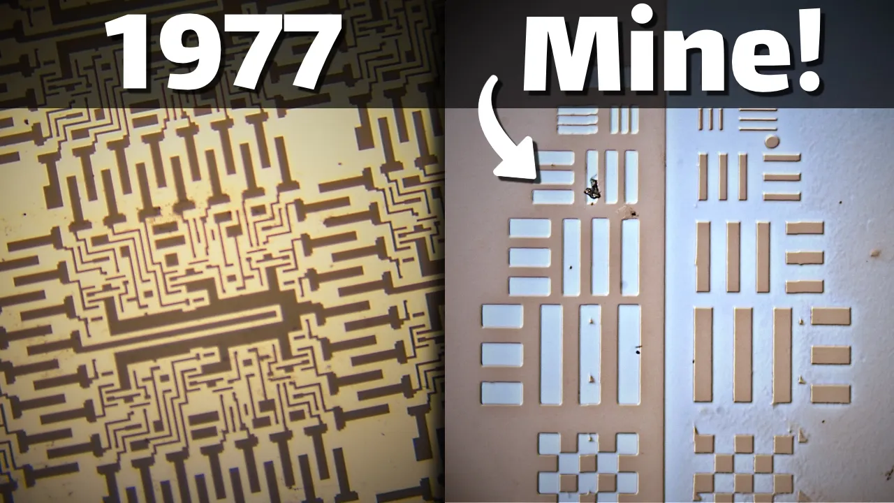
A subtle angular error in the optical head creates slight rotational mismatches between adjacent stepped exposure fields. Although optical calibration routine helped minimize the error, the field boundaries still show step-off seams. Corner vignetting and subtle tip-tilt misalignment also cause periodic underexposed triangular regions along image boundaries, where defocused, diffuse UV light failed to fully clear during chemical development. Compounding this, insufficient soak time in ferric chloride left a faint, foggy veil of unetched copper haze across the central aperture. Finally, an arithmetic error in calculating the micrometers-per-pixel ratio scaled the minimum reticle geometry up to 2 to 3 micrometers instead of the planned 1-micrometer design target.

“The stage is holding great positioning accuracy because it has those, you know, one nanometer encoders on it, but there are still some misalignments if you look closely, and this is actually due to a rotation in the optical system,” he observes.

- **Photomask Media:** Float glass plates coated with ~100 nm of opaque copper, chosen for chemical compatibility with common ferric chloride etchant. - **Encoder Resolution:** 1 nm optical linear encoders on the motion axis maintain stage positioning accuracy across stepped fields. - **Optical Aberrations:** Tip-tilt focal tilt caused exposure drop-off in field corners, while mechanical field rotation generated stitching seams at adjacent sub-field boundaries. - **Scaling Offset:** A pixel-to-micron conversion error caused the smallest chrome/copper features to print between 2.0 and 3.0 µm rather than the nominal 1.0 µm target.

---

[39:57](https://www.youtube.com/watch?v=RuVS7MsQk4Y&t=2397s) First Reduction Exposure Results

Running the flawed copper mask through the reduction stepper yields encouraging proof-of-concept silicon exposures. Because the physical mask features were unintentionally enlarged during maskless synthesis, the projected wafer features scale down to approximately 2.0 to 2.5 micrometers. Central patterns on the exposed wafer exhibit degraded line fidelity directly tracing back to the foggy, under-etched copper haze present on the reticle, but surrounding structures demonstrate crisp edge delineation and clean profile definition.

Field inspection indicates noticeable optical falloff near the peripheral edges of the exposure field, which stems from non-uniform illumination intensity across the condenser beam compared to the center. While increasing exposure durations could partially compensate for this edge roll-off by pushing marginal zones past the photoresist threshold, it highlights the need for uniform light integration. Even with minor imperfections, the reduction optics successfully reproduced sub-3-micrometer structures without mechanical destruction or severe chromatic defocus.

“Hey, I mean, not bad honestly; there are some limitations and problems here, but we knew about those already, like the minimum feature size is about two, two and a half microns due to the mask being scaled a little incorrectly, and the features in the middle are kind of garbage because the mask was kind of garbage there, but generally it turned out really well,” Breaking Taps reports.

---

[40:41](https://www.youtube.com/watch?v=RuVS7MsQk4Y&t=2441s) Blown UV LEDs and Existential Dread

When attempting to produce an optimized, higher-resolution reticle, the maskless exposure system abruptly fails during its boot routine. Troubleshooting the power delivery board reveals that the high-power ultraviolet illumination array has blown. Placing a digital multimeter in diode-check mode across the functioning red LED channel shows a nominal forward drop of 0.6 volts and zero conductivity in reverse bias. Testing the modified blue/UV LED channel, however, returns identical readings of 0.071 volts in both forward and reverse directions, indicating damaged, internally shorted emitter junctions.

Fixing the dead UV source requires a catastrophic teardown: the emitters sit buried behind an integrated heat sink, demanding that the controller PCB, optical rail mounts, and chassis covers all be dismantled to access the bare board. Although spare 365 nm LEDs were on hand as potential replacements for the stock 405 nm emitters, their surface-mount land pattern does not match the driver PCB traces. Though replacement PCBs were fabricated and delivered, the emotional fatigue of endless rebuild cycles halts immediate progress.

“I did end up making those PCBs and I just received them, but I don't know, I feel like this is a natural stopping point for the video, and frankly the prospect of tearing apart the whole optical system for like the 100th time fills me with existential dread,” Breaking Taps admits.

| Diagnostic Channel | Forward Bias Voltage | Reverse Bias Voltage | Component Status | |:--- |:--- |:--- |:--- | | **Red LED Channel** | ~0.60 V | 0.00 V (Open) | Nominal functional diode | | **UV (ex-Blue) Channel** | ~0.071 V | ~0.071 V | Shorted junction / Blown emitter |

---

[42:55](https://www.youtube.com/watch?v=RuVS7MsQk4Y&t=2575s) A Qualified 1980 Win and Structural Steel Fabrications

While the ultimate goal of resolving sub-micrometer geometries was narrowly missed—stabilizing instead between 2.0 and 2.5 micrometers—the project achieved its broader technological milestone. Examining original commercial silicon photomasks from the late 1970s reveals that while critical resolution targets like transistor gate lengths scaled down to 2 or 3 micrometers, the vast majority of interconnects, metal vias, routing traces, and bonding pads were significantly coarser. Constructing a fully functional dual-platform suite—consisting of a maskless pattern generator and a 10:1 reduction optical stepper—effectively replicates industrial semiconductor photolithography capabilities circa 1980 from a home shop.

“Chips might need the finest resolution for certain areas like the transistor channels, but for the most part most things on a chip are actually pretty big—all the wiring and vias and contact pads—so I'm going to personally count this as a qualified win,” Breaking Taps concludes.

Closing reflections turn to machine design and sponsor SendCutSend, whose on-demand sheet metal laser cutting and CNC bending allowed the structural baseplates to be fabricated cheaply and rigidly. Outsourcing quarter-inch-thick steel sheet fabrication avoided the logistical nightmare of personal material handling, where a single raw 4×8-foot plate weighs roughly 600 pounds, retails around $700, and incurs hundreds more in freight charges. Relying on precision-folded commercial sheet parts ensured structural stability across both stepper chassis without overburdening a home workshop.

[44:58](https://www.youtube.com/watch?v=RuVS7MsQk4Y&t=2698s) Sheet Metal Learnings and Future Technical Deep Dives

Reflecting on the fabrication process, Breaking Taps remarks on the sheer heft of ordering quarter-inch thick steel, noting that the sheer mass made free shipping a particularly welcome bonus. Beyond the convenience, learning how to properly design for and assemble bent sheet metal proved to be an exciting new capability to add to the workshop toolkit, opening up plenty of ideas for subsequent builds. Breaking Taps enthusiastically endorses using SendCutSend for rapid sheet metal prototyping: “If you are working on a project that could benefit from sheet metal, I highly recommend checking out SendCutSend; it was super easy and the parts were great.”

Despite the primary video running quite long, a substantial amount of deep technical material had to be trimmed in the editing room to keep the overarching narrative manageable. Fascinating topics like precision motion systems, kinematic mounts, software compensation, and intricate optical alignment ended up on the cutting-room floor. To ensure these granular insights are not lost, Breaking Taps plans to release a looser, more casual companion video: “So the plan is to edit together kind of an engineering cut of all the extra details and footage that didn't make this one and just do a kind of, you know, low production value stream of conscious looking at a webcam sort of thing, and that'll be out in I don't know, a week or three, whenever I recover from editing this one.”

- **Heavy materials:** The initial order featured quarter-inch thick steel plate components, resulting in a remarkably heavy shipping box. - **Companion engineering cut:** An unpolished, webcam-style deep dive will cover the specialized technical details cut from the main video, specifically focusing on kinematics, stage motion, error compensation, and optics.

## Notable quotes > [42:55](https://www.youtube.com/watch?v=RuVS7MsQk4Y&t=2575s) Chips might need the finest resolution for certain areas like the transistor channels, but for the most part most things on a chip are actually pretty big—all the wiring and vias and contact pads — Breaking Taps

## Mentioned Breaking Taps, SendCutSend, GCA Corporation, GCA Mann 4800 DSW, Texas Instruments, HackerFab, Carnegie Mellon University, Sam Zeloof, Huygens Optics, Autodesk Fusion 360, Zaber Technologies, Zaber X-ADR, Carl Zeiss, Zeiss S-Planar

## Video description Try SendCutSend 15% off for your next project! https://sendcutsend.com/breakingtaps/

My descent into madness, chasing one micrometer.

Watch this ad-free on Nebula: https://nebula.tv/videos/breakingtaps-speedrunning-30yrs-of-semiconductor-history

🥰 CONSIDER SUBSCRIBING 🥰 🔬Patreon if that's your jam: https://www.patreon.com/breakingtaps

📢Twitter: https://twitter.com/BreakingTaps 📷Instagram: https://instagram.com/breakingtaps 💻Discord: https://discord.gg/R45uCXcEv4

=== Links === - Zaber X-ADR stage: https://www.zaber.com/products/scanning-microscope-stages/X-ADR-AE?utm_source=youtube&utm_campaign=breaking-taps

- HackerFab: https://hacker-fab.gitbook.io/hacker-fab-space - Sam's Stepper: https://www.youtube.com/watch?v=Nxz_ENnmgtI - Huygens Optics' Stepper: https://www.youtube.com/watch?v=MdRwiI6VLmk

- Zeiss S-Planar info (Search for "micro-lithography" to find the section): http://www.marcocavina.com/articoli_fotografici/Zeiss_cute_DFR_DDR_lenses/00_pag_English.htm - GCA Mann 4800 DSW: https://www.chiphistory.org/99-gca-mann-4800-direct-step-on-wafer-system

- "Development of a quasi-collimated UV LED backlight for producing uniform and smooth 3D printing objects": https://opg.optica.org/oe/fulltext.cfm?uri=oe-30-9-14759&id=471540

=== Timeline ===  0:00 Intro 3:04 Ch. 1 - Structure 9:08 Ch. 2 - Assembly 20:07 Ch. 3 - Pain 24:25 Ch. 4 - Existential Crisis 37:11 Ch. 5 - Salvation?

[Source](https://www.youtube.com/watch?v=RuVS7MsQk4Y)

中文简报

Breaking Taps自制两级步进光刻机,实现2微米芯片特征图案打印 由于高倍率光学元件在手动定位平台上缺乏足够的景深,直写无掩模光刻在拼接曝光中失败,迫使作者改用两级缩印工作流以稳定达到1980年代的芯片分辨率。 为了复现1978年GCA Mann 4800等工业级步进光刻机具有里程碑意义的1微米制程能力,Breaking Taps基于改造型德州仪器DMD投影仪和高精度Zaber移动平台,设计并制造了一台无掩模光刻机。然而,极浅的景深和光刻胶附着力问题使得在晶圆上直接直写图案难以实现,他随后转向打造一台完全独立的第二代设备:基于老式蔡司缩印镜头和自制准平行紫外光源构建的10:1晶圆步进光刻机。该两级工作流利用无掩模光刻机制作铜质掩模版,再通过步进光刻机曝光硅衬底,克服了重大的机械与对准难题。尽管像素缩放误差和紫外LED烧毁将最终分辨率限制在2.0至2.5微米,但该实验成功证实了在车库中复刻约1980年代水平微加工工艺的可行性。 Breaking Taps尝试在家庭工作室使用现成零件复刻1978年时代的1微米半导体光刻技术,参考了GCA Mann 4800 DSW等价值数百万美元的历史机型。 (0:00) 受限于高数值孔径直写光学元件的景深限制及焦点漂移,该项目转向两级方案:先用DMD无掩模引擎光刻掩模版,再通过老式蔡司10:1缩印镜头将其曝光到晶圆上。 (24:25) 自制的晶圆步进光刻机采用了结合毛玻璃扩光片、增亮膜(BEF)和微百叶窗防窥片的薄膜准平行紫外光源,无需庞大的聚光镜组即可实现定向照明。 (30:08) 尽管紫外LED烧毁和光掩模缩放误差导致最终测试提前终止,该装置仍展现出2.0至2.5微米的可分辨硅结构,实际上达到了约1980年商用半导体制造的水平。 (42:55)

Reading summary

Breaking Taps set out to replicate industrial circa-1978 photolithography in a home workshop, attempting to achieve 1-micrometer feature resolution using modern off-the-shelf components and digital maskless projection. Adapting DLP Projection for Maskless Photolithography (4:41) Rather than constructing a direct-write laser scanning rig, the project implemented a digital maskless architecture using a Texas Instruments Digital Micromirror Device (DMD) development kit. Drawing inspiration from open-source microfabrication efforts like Carnegie Mellon University's HackerFab, this approach eliminated physical photomasks by rendering digital patterns directly onto the micromirror array. To match photoresist actinic sensitivity, the projector's stock blue LED was desoldered and replaced with a ultraviolet (UV) LED, while the original red and green LEDs were retained to enable non-actinic alignment and inspection. The optical train directed UV light from the DMD through a collimating lens, a beam splitter cube, and an infinity-corrected microscope objective to focus patterns onto the substrate. Light reflecting from the substrate returned through the objective and beam splitter into an alignment camera. For multi-axis positioning, the optical column was paired with an industrial Zaber XY motion stage featuring 1-nanometer resolution optical encoders, 50-nanometer minimum incremental motion, and calibrated pitch and yaw compensation, seated beneath a custom rotary vacuum chuck. Mechanical Stackup and Focal Depth Bottlenecks (19:04) Initial exposure tests quickly encountered physical limitations imposed by high-magnification optics. Although a high numerical aperture (NA) objective could theoretically resolve features down to roughly 800 nanometers, its microscopic depth of field proved incompatible with manual stage leveling. Scanning electron microscope (SEM) inspections revealed that while isolated features resolved, neighboring exposure fields were smeared and improperly exposed due to vertical focal drift. Measurements using a dial test indicator revealed substantial geometric runout accumulated across the homemade mechanical stackup. The rotary spindle showed 0.004 inches (~100 µm) of total indicator reading caused by spindle inaccuracies and platen wobble, an oversized vacuum O-ring rocked the kinematic mount, and the Y-axis displayed roughly 0.003 inches (~76 µm) of continuous incline. Although adding 0.005 inches of precision brass shims reduced local variations to between 2.5 and 5.0 µm, the system could not maintain focus across large, stitched exposure fields. Furthermore, aged photoresist from around 2018 routinely delaminated from bare glass upon solvent development. Pivoting to a Two-Stage Optical Stepper (24:25) To circumvent the unforgiving depth of field of high-NA direct writing, Breaking Taps shifted to a two-stage reduction strategy mirroring historical semiconductor manufacturing. Swapping the primary tool to a low-magnification 4X objective relaxed the depth of field, enabling it to function reliably as a reticle generator for 10- to 20-micrometer features. These reticles were then projected onto silicon using a newly built second machine: a dedicated wafer stepper centered around a late-1970s vintage Zeiss S-Planar 10:1 reduction lens originally manufactured for early commercial steppers like the GCA Mann 4800 DSW. Illumination for the stepper required quasi-collimated light, achieved through an optical sandwich inspired by 3D printer backlights: a sandpaper-etched ground glass diffuser, two orthogonally crossed Brightness Enhancing Films (BEF) that recycle wide-angle rays, and two crossed micro-louver privacy filters that absorb stray off-axis light. For layer registration, an all-metal alignment train used a beam splitter above the Zeiss lens and a reversed microscope objective on an XYZ translation stage, projecting conjugate images of the mask and wafer directly onto a camera sensor. Fabrication Results and Electrical Failure (37:42) Photomasks were fabricated by sputter-coating float glass with approximately 100 nanometers of opaque copper and etching the exposed patterns in ferric chloride. The synthesized masks suffered from minor optical rotation seams, corner underexposure from tip-tilt errors, central copper haze from insufficient etching, and a pixel-scaling error that enlarged base features to 2 to 3 micrometers. When run through the 10:1 reduction stepper, the setup successfully resolved features between 2.0 and 2.5 micrometers on silicon with clean boundary profiles, despite optical falloff at peripheral field edges. Subsequent attempts to produce higher-resolution reticles ceased when the maskless projector's UV LED array failed during boot. Diode-check diagnostics confirmed an internal electrical short, showing matching 0.071-volt drops in both forward and reverse bias across the modified UV channel, compared to a normal 0.60-volt forward drop on the functional red channel. Facing another total teardown of the buried heatsink assembly, Breaking Taps concluded testing. Although the project missed its original 1-micrometer target, stabilizing at 2.0 to 2.5 micrometers, Breaking Taps characterized the outcome as a qualified win that successfully replicated circa-1980 commercial microfabrication capabilities. Replacing bespoke machinery with folded sheet metal chassis, precision outsourced fabrication, and legacy reduction optics demonstrated that multi-million-dollar historical lithography workflows can be approximated in a home workshop.

精炼阅读摘要

自制创客频道 Breaking Taps 尝试在个人车间复刻 1978 年工业级 1 微米半导体光刻工艺;在直写模式遭遇光学焦深极限与机械累计公差瓶颈后,他将方案调整为由“无掩模光罩生成机”与“10:1 光学缩减步进机”构成的双机架构,最终在硅片上实现了 2.0 至 2.5 微米特征尺寸的曝光验证。 历史基准与无掩模光刻平台的初步构建 (0:00) 半导体产业在 1978 年实现了 1 微米特征尺寸的集成电路量产,当时高度依赖价值约 45 万美元(折合现代约 200 万美元)的工业级设备,其代表机型为首台商用光学缩减晶圆步进光刻机 GCA Mann 4800 DSW。为低成本复刻该能力,Breaking Taps 放弃了存在大面积拼接误差的电子束光刻(EBL)与激光直写路线,借鉴卡内基梅隆大学 HackerFab 等开源项目的架构,采用德州仪器(TI)数字微镜器件(DMD)投影芯片构建数字化无掩模光刻系统,以计算机渲染画面完全取代实体物理掩模。 在机械构建上,系统放弃了传统的铝挤型材与 3D 打印件,通过 Autodesk Fusion 360 设计了定制的 A36 软钢与冷轧钢折弯钣金机箱,并交由 SendCutSend 加工,以抑制微米级曝光下的环境振动。运动核心采用了 Zaber 赞助的工业级 XY 线性平台,具备 1 纳米分辨率光学编码器与 500 纳米双向重复精度。光学引擎拆解改装自 TI DLP 评估套件,将原有蓝色 LED 换焊为光刻胶敏感的紫外(UV)LED,保留红绿 LED 用于安全对准检查,光束经准直透镜、分光棱镜及高数值孔径无限远校正显微物镜聚焦至真空吸附旋转卡盘上的基底。 焦深物理瓶颈迫使向双阶段微缩架构转向 (24:25) 在玻璃基底上的直接曝光测试显露出两大物理障碍。首先是工艺材料问题:所用的光刻胶已于 2018 年左右过期,表面附着力严重衰减,溶剂显影穿透至玻璃界面时图案发生整片剥离脱落;其次是严苛的景深限制。高数值孔径(NA)物镜虽然理论上能解析约 800 纳米的结构,但焦深极其微小,基底表面轻微的起伏即可导致焦点脱靶。 千分表检测暴露出自制机械堆叠累积的严重形位误差:旋转主轴存在约 0.004 英寸(约 100 微米)的全跳动误差,Y 轴滑移全程呈现约 0.003 英寸(约 76 微米)的连续倾角,且过大的真空密封 O 型圈妨碍了运动学卡盘的平稳落座。在缺乏闭环电动 Z 轴自动对焦的情况下,即使塞入精密黄铜垫片反复调平,也无法支撑大面积拼接曝光。作者因此放弃了单一直写方案,启动两阶段的“Plan B”:改用景深容差更大的 4X 低倍物镜将无掩模系统降级为光罩生成机,仅写入 10 至 20 微米的光罩结构;随后另建一台专用的 10:1 光学缩减步进光刻机,将光罩图案二次微缩至最终硅片上。 步进机薄膜准直光引擎与全金属对准机构 (28:18) 独立步进光刻机底盘采用对称零件设计,使激光切割钣金的外包成本降低了 20% 至 30%。缩减物镜采用了作者此前在 eBay 购入的 1970 年代末蔡司 S-Planar 10:1 工业镜头,该镜片历史上曾装配于早期的 GCA Mann 4800 步进机。为解决步进光刻所需的平行光照明难题,作者借鉴 3D 打印机背光方案设计了一套薄膜准直 UV 光引擎:将毛玻璃扩散片、两层相互正交的微棱镜增亮膜(BEF)与两层微百叶窗防窥膜相互层叠,利用全内反射回收杂光并由百叶窗吸收大角度偏折光,以显著的光强衰减代价换取高方向性的准直 UV 光束。 针对掩模与基底套刻,初期基于 3D 打印支架与普通变焦镜头的对准光路因成像模糊宣告失败。作者将其全面改版为机加工铝合金与钣金结构,采用分光棱镜配合反向显微物镜将反射图像缩放至相机传感器。该对准模组配备了三自由度位移台:Y 轴线性滑台用于共轭调焦,X 与 Z 轴用于平移扫描掩模各区域的对准标记。操作人员可在非感光的红光照明下使掩模与晶圆特征同时合焦并校准,随后滑入 UV 光引擎完成曝光。 铜光罩制备、曝光验证与合格的技术突破 (37:42) 在光罩制作环节,作者在浮法玻璃上溅射约 100 纳米厚的金属铜层作为遮光介质,使用无掩模光刻机曝光后以三氯化铁溶液腐蚀成形。尽管 Zaber 平台的 1 纳米编码器提供了可靠的步进定位,但光路微小的装配倾角导致视场边界存在微小旋转缝隙,边缘渐晕引发了局部欠曝,腐蚀时长不足在中心区留下了未蚀刻透的铜雾,且像素换算错误直接将掩模最小尺寸放大了 2 至 3 微米。 将该铜掩模装入步进机曝光后,硅片成功显影出 2.0 至 2.5 微米的结构轮廓。中心区域因掩模铜雾出现线条退化,视场边缘也显现出照度滚降引起的曝光不均,但整体图案边缘清晰。在着手优化光罩时,无掩模光刻机的 UV LED 阵列在开机中烧毁,万用表测试显示其正反向导通压降均为 0.071 伏(正常红光 LED 为正向 0.60 伏、反向截止),证实芯片内部已短路击穿。作者总结认为,尽管未能突破 1 微米这一最初指标,但考虑到 1980 年代初期的芯片多仅在晶体管栅极处采用 2 至 3 微米线宽,其余布线与焊盘均远为粗大,在车间内完整跑通此套光刻全流程仍属于一次合格的突破。 该项目证明了个人工坊利用现代数字化设计、外包钣金与二手工业级光学元件复刻早期工业微米级光刻的可行性。系统的核心局限依然在于高倍物镜景深与机械平整度之间的结构性矛盾、过期化学品的工艺缺陷,以及改装电子元件的热电可靠性。作者表示后续将整理未剪辑的工程深潜视频,进一步公开精密运动平台、运动学卡盘与光学调试等具体细节。

Detailed notes — zh

## Background 该内容由 YouTube 创作者 Breaking Taps 于 2024 年 7 月 31 日发布。视频页面描述将其概括为“一场追逐 1 微米精度的癫狂之旅”,记录了博主试图在个人车间内以远低于工业设备的成本,挑战复刻过去 30 年半导体光刻演进历程的硬核造机过程。 ## TL;DR 为了在个人车间复刻价值 200 万美元的 1978 年 GCA Mann 4800 分步重复光刻机并冲击 1 微米特征尺寸,博主首先利用德州仪器 DMD 芯片与高精度 Zaber 位移台搭建了一台无掩模光刻机。在遭遇钣金翘曲、公差累积失焦、光刻胶附着力失效以及高数值孔径景深过浅等连环工程挫折后,他转向“方案 B”,自制了一台搭载 1970 年代蔡司 10:1 缩写物镜的投影步进光刻机,并辅以自制的无掩模设备光刻制作铜薄膜掩模版。尽管因紫外 LED 突发短路烧毁、掩模尺寸换算失误等原因最终停留在 2 至 2.5 微米的分辨率,未能严格达成 1 微米指标,但博主成功验证了整套两级光刻方案,实现了相当于 1980 年代工业水准的芯片制造能力。 ## Atmosphere & style 视频兼具硬核工程极客的严密求真与 DIY 创客自嘲式的黑色幽默,将一场雄心勃勃的技术“速通”拍成了跌宕起伏的排障长征。博主面对钣金变形、机械干涉、千分表打表调平以及核心元器件突发烧毁时,流露出真实而深切的技术窒息感与存在主义疲惫。观感既像是在见证一场充满精密机械与光学魅力的微观工艺冒险,又让人对半导体工业背后令人发指的物理公差极限产生由衷的敬畏。 ## Bulletin - [00:00](https://www.youtube.com/watch?v=RuVS7MsQk4Y&t=0s) 博主 Breaking Taps 尝试在个人工作室复刻 1978 年价值约 200 万美元的半导体光刻能力,挑战在无需昂贵物理掩模的前提下实现 1 微米特征尺寸的大面积曝光。 - [23:23](https://www.youtube.com/watch?v=RuVS7MsQk4Y&t=1403s) 首台设备基于德州仪器 DMD 芯片和 Zaber 高精度纳米位移台构建无掩模光刻机,因高 NA 物镜景深极浅叠加机械公差累积,导致无法在多视场拼接下维持全域对焦。 - [24:25](https://www.youtube.com/watch?v=RuVS7MsQk4Y&t=1465s) 面对景深瓶颈,作者转向“方案 B”,用低倍物镜无掩模制作 100 nm 铜层掩模版,再交由 1970 年代末蔡司 10:1 缩减物镜步进投影,成功打通微缩光刻物理流程。 - [40:41](https://www.youtube.com/watch?v=RuVS7MsQk4Y&t=2441s) 因紫外 LED 内部短路烧毁且整机拆修难度极大,项目在达到 2 至 2.5 微米分辨率时告一段落,虽未达 1 微米指标,但已具备完整制造 1980 年代芯片的物理能力。 ## Key takeaways - [00:00](https://www.youtube.com/watch?v=RuVS7MsQk4Y&t=0s) 以 1978 年 GCA Mann 4800 DSW 分步光刻机为标杆,项目确立了攻克 1 微米特征尺寸与大面积稳定光刻的两大核心目标。 - [03:04](https://www.youtube.com/watch?v=RuVS7MsQk4Y&t=184s) 机身结构放弃铝型材,改用 1/4 英寸 A36 碳钢板与折弯钣金,虽因热轧残余应力发生翘曲,但三维立柱锁紧后提供了极高的抗微振刚性。 - [04:41](https://www.youtube.com/watch?v=RuVS7MsQk4Y&t=281s) 光学核心采用 TI DLP 投影仪开发套件,拆卸原装放映镜头并换装 UV LED,通过反向显微缩减光学实现数字调制的无掩模光刻。 - [10:33](https://www.youtube.com/watch?v=RuVS7MsQk4Y&t=633s) 位移系统采用配备 1 nm 分辨率编码器与 50 nm 步进的 Zaber XY 线性台,但上层叠加的主轴、O型圈与微调台带来了高达数千分英寸的累积倾斜误差。 - [20:08](https://www.youtube.com/watch?v=RuVS7MsQk4Y&t=1208s) 通过千分表反复打表并在底板两角塞入 0.005 英寸金属精密垫片,作者将横向全行程平移倾斜压缩至约 2.54 微米(1 个 Tenth),勉强适配焦深极限。 - [23:23](https://www.youtube.com/watch?v=RuVS7MsQk4Y&t=1403s) 2018 年过期的老旧光刻胶在显影液穿透到底部时会迅速整片剥离,化学附着力退化成为限制微观成型的关键因素之一。 - [23:23](https://www.youtube.com/watch?v=RuVS7MsQk4Y&t=1403s) 高数值孔径(High NA)物镜的焦深极度狭窄,现有手动 Z 轴平台无法克服微小机械倾角,成为无掩模直接光刻无法逾越的物理瓶颈。 - [24:25](https://www.youtube.com/watch?v=RuVS7MsQk4Y&t=1465s) 技术路线转向“方案 B”:用大景深低倍物镜制造大尺寸掩模,再通过蔡司 10:1 缩写物镜将图案缩微投射到晶圆上,复刻半导体工业经典路线。 - [30:08](https://www.youtube.com/watch?v=RuVS7MsQk4Y&t=1808s) 缩写光刻机引入由毛玻璃扩散板、两层正交增亮膜(BEF)及两层正交防窥膜构成的薄膜光学堆叠,实现高准直度的平行 UV 背光输出。 - [32:47](https://www.youtube.com/watch?v=RuVS7MsQk4Y&t=1967s) 为解决显微套刻对准问题,设备彻底弃用 3D 打印件并改用全金属加工,在基底承载端集成了支持角度补偿的 XY-Z-θ 四轴对准载物台。 - [34:19](https://www.youtube.com/watch?v=RuVS7MsQk4Y&t=2059s) 对准光路通过反向安装的显微物镜聚焦至相机,并通过直接拆卸物镜前半段金属外壳解决了与相机 C 口螺纹孔的几何干涉问题。 - [37:12](https://www.youtube.com/watch?v=RuVS7MsQk4Y&t=2232s) 正式掩模采用玻璃基底溅射 100 nm 铜层制成,该厚度兼具光学不透明性与氯化铁腐蚀液中快速溶解剥离的特性。 - [38:04](https://www.youtube.com/watch?v=RuVS7MsQk4Y&t=2284s) 显微质检发现首张铜掩模存在微小视场旋转、倾角导致的边缘三角形失焦、显影不足导致的中心残铜,以及像素换算失误等瑕疵。 - [39:57](https://www.youtube.com/watch?v=RuVS7MsQk4Y&t=2397s) 使用该掩模进行 10:1 缩减曝光成功得到了 2 至 2.5 微米的特征尺寸,验证了整套微缩步进光学系统的物理可行性。 - [40:41](https://www.youtube.com/watch?v=RuVS7MsQk4Y&t=2441s) 无掩模光刻机的紫外 LED 突发短路击穿,由于光学架构深度嵌套导致维修拆机成本极高,加之作者精力耗尽,未展开二次迭代。 - [42:41](https://www.youtube.com/watch?v=RuVS7MsQk4Y&t=2561s) 最终成果被定为“有条件的胜利”:自制设备虽未击穿 1 微米目标,但其实际制造能力已完全足以复刻 1980 年代工业水准的经典半导体芯片。 ## Detailed walkthrough ### [00:00](https://www.youtube.com/watch?v=RuVS7MsQk4Y&t=0s) 挑战 1 微米特征与 200 万美元的工业历史 从 1947 年人类制造出第一只晶体管,到 1978 年半导体工业已经能够制造出特征尺寸仅为 1 微米(1 µm)的集成电路。1 微米大约只有人类头发直径的五十分之一,在当年实现这一精度的工业级设备造价高达约 200 万美元(以如今货币折算)。Breaking Taps 决定在自己的个人工作室中复刻这一制造能力,打造一台能达到 1 微米分辨率的光刻机。博主打趣道,现在已经是 2024 年,他完全可以利用现代技术“作弊”,以“速通”(Speedrun)的方式跨越过去 30 年的半导体技术演进,同时将制造成本压低到远低于 200 万美元的水平。 制造集成电路通常包含数百道工序,但其中最核心的步骤非光刻(Photolithography)莫属。光刻的本质是将设计好的微缩图案转移到涂敷在晶圆表面的光刻胶(光敏树脂)上,随后的所有刻蚀、掺杂等工序都依赖于该图案。这一原理与胶片相机曝光乳胶、SLA 3D 打印机固化树脂,或者制造 PCB 电路板所用的光阻完全一致,唯一的根本差异在于微观尺度。芯片结构极小,因此投射到芯片表面的图案也必须极其微小。 在此之前,博主曾做过几台简易设备,但用他自己的话来说:“坦率地讲,那台机器不太行,除了拿来当原理演示外基本上无法实用。”他也尝试过电子束光刻(Electron Beam Lithography, EBL),虽然该方案极擅长制作纳米级超微结构(例如他制作的几百纳米间隙真空晶体管),却极其不擅长进行大面积曝光。在之前制作 DIY 相机传感器的项目中,多视场视场拼接(Stitching)带来的累积误差让他吃尽了苦头。因此,该项目确立了两个核心目标: - **攻克 1 微米特征尺寸**:这不仅是一个整洁好看的数字,更契合了芯片工业的历史转折点。1978 年,GCA 公司推出了商业上大获成功的 GCA Mann 4800 DSW(Direct Step on Wafer)分步重复光刻机,该设备首次采用缩减物镜将掩模图案缩小并投影在晶圆上,售价为 450,000 美元(约合现今 200 万美元)。博主直言:“在自己的工作室里做出一台价值 200 万美元机器的等效设备,听起来就是一个很有意思的挑战。” - **在大面积区域内稳定光刻**:用高质量显微镜物镜在极小局部做出亚微米结构并不罕见,但要在大视场范围内稳定、均匀且一致地打印出这种精细结构,工程难度极高。 --- ### [03:04](https://www.youtube.com/watch?v=RuVS7MsQk4Y&t=184s) 结构设计:告别铝型材与钣金折弯实践 回顾几年前制作的第一代简易光刻设备,整体结构仅由铝型材、3D 打印件以及“基本上像泡泡糖一样脆弱的连接”拼凑而成,完全是边做边搭。为了让新机器具备真正的工业可靠性与刚性,博主打开 Fusion 360,“假装自己是一个正经工程师”来开展严格的 CAD 建模。整个机身框架不仅承担着机械支撑的作用——底部安装高精度移动台,顶部悬挂精密光学系统——还要兼作光刻机的避光外罩。光刻胶对紫外光极度敏感,因此框架表面嵌有大面积的黄色亚克力滤光板,用以阻隔外界一切可能导致光刻胶提前曝光的光线。 在结构选材上,博主放弃了常见的 8020 铝型材,也排除了廉价木板方案,首次决定采用钣金件(Sheet Metal)。他认为 8020 铝型材组装和调平非常繁琐,而钣金既专业又紧凑。由于个人车间里的 CNC 雕刻机无法加工大幅面板材,他选择将 CAD 导出的 DXF 和 STEP 文件发送给在线激光切割加工商 SendCutSend。借由 Fusion 360 的钣金模块,输入加工商提供的折弯扣除参数,直接设计了大量的冲压折弯与翻边结构,大幅减少了紧固件数量与后续组装难度。 ```mermaid flowchart TD accTitle: 光刻机整机结构与防护布局 accDescr: 展示光刻机顶部光学系统、底部工件台以及外围黄色亚克力防紫外外壳的机械架构关系。 subgraph Enclosure["防护与支撑框架 (钣金结构)"] direction TB Panels["黄色防紫外亚克力窗\n(滤除 UV 光保护光刻胶)"] Frame["1/4 英寸 A36 碳钢底板\n+ 冷轧钢/铝侧壁箱体"] end subgraph CoreComponents["核心工作单元"] Optics["顶部: DMD 无掩模光学投影与对准系统"] Stage["底部: 高精度多轴移动台 (承载晶圆片)"] end Frame --- Optics Frame --- Stage Panels -.->|"外围包裹封闭"| Frame ``` --- ### [04:41](https://www.youtube.com/watch?v=RuVS7MsQk4Y&t=281s) 光路构想:基于德州仪器 DMD 的无掩模光刻引擎 整台机器的光学核心取材于德州仪器(Texas Instruments)的 DLP 投影仪开发套件。开发板原本包含三个部分:前置投影镜头、DMD 芯片本体,以及一套由多组复杂透镜构成的照明引擎,用于将红、绿、蓝三色高功率 LED 耦合进光路。为了实现光刻功能,博主要做的改造是:拆卸原装投影镜头并安装自定义转接环以配合显微镜缩减光学;保留原装红、绿 LED 用于芯片对准、检测与找焦,而将原厂的蓝光 LED 拆除,手工更换为高能量紫外(UV)LED。 博主拆解了无掩模光刻(Maskless Lithography)的底层工作原理: DMD 内部集成了成千上万个微型可翻转反光镜(Micro Mirrors)。每个微镜由数字信号独立寻址,当镜片向一个方向偏转时,光线被反射进入光路物镜形成亮像素;向另一方向偏转时,光线被导向光阱偏离主光路,形成暗像素。如果拆下原有的放大放映镜头,反向接入一组光学缩减系统(如高数值孔径显微镜物镜),就能把计算机中任意绘制的数字图形以极高倍率缩小并清晰成像在晶圆上。这一方案免去了动辄数千美元制作物理掩模版(Photomask)的成本,是学术界与工业界非常成熟的研究路线。博主提到,CMU 的开源硬件学生组织 HackerFab 以及 YouTube 上的博主 Sam、Huygens Optics 等此前都制作过类似方案,而 HackerFab 详尽的开源文档更是为他选型 DMD 提供了宝贵参考。 ```mermaid flowchart LR accTitle: DMD 无掩模共焦光路拓扑 accDescr: 展示从 UV/RGB 光源经 DMD 反射、平行准直、分光镜分光到显微物镜聚焦,并经同轴反射回到对准相机的光路传播机制。 subgraph Illumination["照明引擎"] LED["UV / 绿 / 红 LED 光源"] -->|"均匀照明"| DMD["TI DMD 芯片\n(微镜数字调制图形)"] end subgraph OpticalTrain["物镜缩减与成像光路"] DMD -->|"发散图案光束"| L1["第一准直透镜"] L1 --> BS["分光棱镜 (Beam Splitter)"] BS -->|"透射主光路"| Obj["显微物镜 (Reduction Optics)"] Obj --> Wafer["硅片表面光刻胶"] end subgraph InspectionArm["同轴检测与对焦光路"] Wafer -.->|"基底反射光"| Obj Obj -.-> BS BS -->|"90度反射"| L2["成像镜"] L2 --> Cam["USB 对准相机"] end ``` 详细的光路物理走向如下: 1. **图形生成与准直**:UV 光源照射 DMD 表面,反射生成的发散图像光束穿过第一组透镜被准直为平行光束。 2. **同轴下行曝光**:平行光穿过 50:50 分光棱镜(Beam Splitter),大部分光线垂直向下进入高倍显微镜物镜,聚焦缩微打在晶圆基底的光刻胶上。 3. **同轴反射与监测**:小部分光线被硅片反射后沿原路返回物镜,到达分光棱镜时被折射 90 度进入水平旁路,通过透镜汇聚在 USB 相机芯片上,实现亚微米级的同轴对焦与视场图形套刻对准。 --- ### [08:45](https://www.youtube.com/watch?v=RuVS7MsQk4Y&t=525s) 焊接改造与机箱装配中的钣金变形教训 在硬件动手阶段,博主必须对 LED 板进行热风拆焊与重构。由于此前从未使用过锡膏(Solder Paste),焊接过程略显狼狈:“我以前从没用过锡膏,所以请原谅我接下来要犯下的罪过。”虽然高功率紫外 LED 被焊得有些歪斜,但万幸经过万用表和点亮测试后电气性能完全正常。紧接着,博主在 DMD 底座安装板上打孔攻丝,完成准直管与笼架系统(Cage System)的同轴装配。 数天后,激光切割零件送达,机架组装正式展开。为了追求绝对的结构刚性以扼杀微振动——振动哪怕只有微米级别也会彻底毁掉光刻分辨率——博主下猛料采用了 1/4 英寸(约 6.35 mm)厚的 A36 低碳钢板作为底板骨架,两侧检修门采用稍薄的冷轧钢板,背板则使用极薄的铝板降低重量。 然而在拼装底板时,博主遭遇了钣金制造的经典翻车案例:1/4 英寸厚的 A36 碳钢底板出现了明显的向上弓形翘曲(Bowing)。博主反思道,这并非激光切割加工商的过错,而是厚钢板自身热轧残余应力的物理天性,从金属批发商买来时就是如此。他剖析了正确的机械设计方案: - **设计缺陷**:底板作为一整块平板没有足够的惯性矩抵抗残余应力变形。 - **改进方式**:本应在底板左侧和前侧设计向上翻折的折弯凸缘(Flanges),将平板变成类似托盘的立体三边或四边“盒子”构型。视频中博主展示了另一块带有两侧折边的小钣金件,其表面呈现出不可思议的平整度。 好在将机架的侧壁和立柱完全拧紧锁合后,三维立体结构强行拉住并约束了底板变形,整体框架恢复了足够的刚性和平直度。博主得以长舒一口气,继续投入下一步的核心部件集成。 ### [10:33](https://www.youtube.com/watch?v=RuVS7MsQk4Y&t=633s) 钣金后处理与 Zaber 高精度位移台 为了给喷漆做准备,所有激光切割板件边缘的毛刺都必须彻底清理干净。虽然激光切割件比等离子切割要干净得多,但仍残留着锐利的毛刺需要打磨。SendCutSend 本身提供了价格非常合理的去毛刺服务,“事后想来,我真应该加购那项服务”,作者感叹道,在自己的小型台式抛光机上给所有零件去毛刺耗费了大量时间,而且效果也不算理想。打磨完后,还必须对所有表面进行脱脂处理,特别是表面涂有防锈油的低碳钢板,随后才能进行底漆与面漆喷涂。作者同样后悔没有直接选用 SendCutSend 的粉末喷涂服务,否则不仅漆面质感会好得多,还能把精力省下来投入到机械结构的其他部分。 在等待油漆风干的同时,作者展示了整台设备的核心运动平台——来自 Zaber 的 XY 线性位移台。“这个令人愉悦的装备是来自 Zaber 的 XY 位移台,说实话,它正是我最初决定开启这个项目的根本原因。”该位移台配备了 1 纳米分辨率的光栅编码器,各项硬件指标堪称惊人:步进分辨率达到 50 纳米,运动重复定位精度达 500 纳米,最大运行速度高达 750 mm/s(接近每秒一米);此外每台设备都附带完整的干涉仪测量数据,详细标定了俯仰(pitch)与偏航(yaw)误差,并可通过完善的 Python API 进行编程控制。作者坦陈该设备由 Zaber 无偿赞助给频道,但对方并非本期视频的商业赞助商,未提前审阅脚本,也无权进行任何内容干预。 - 编码器分辨率:1 nm - 步进增量(Step size):50 nm - 重复定位精度(Repeatability):500 nm - 最大平移速度:750 mm/s - 控制接口:具备完整干涉测量标定数据的 Python API ```mermaid flowchart TD accTitle: Motion Platform Assembly Stack accDescr: Diagram illustrating the layer-by-layer mechanical stack from base stage up to the wafer chuck. subgraph Base ["运动基座"] ZABER["Zaber 高精度 XY 线性位移台\n(1 nm 编码器, 50 nm 步进)"] ADAPT["铝制转接安装板\n(填补中空透射孔)"] ZSTAGE["手动微调 Z 轴升降台"] end subgraph Upper ["承载与旋转结构"] MOTOR["步进电机基座"] SPINDLE["空心回转主轴与真空密封腔\n(带双 O 型圈密封)"] KINEMATIC["磁吸预紧运动学卡盘\n(定位销 + 钢珠)"] CHUCK["晶圆吸盘表面\n(承载曝光基底)"] end ZABER --> ADAPT ADAPT --> ZSTAGE ZSTAGE --> MOTOR MOTOR --> SPINDLE SPINDLE --> KINEMATIC KINEMATIC --> CHUCK ``` ### [12:35](https://www.youtube.com/watch?v=RuVS7MsQk4Y&t=755s) 晶圆吸盘旋转机构与装配失误修正 Zaber 这款位移台最初是为倒置显微镜设计的,因此中心留有大面积透光中空区域;由于本项目采用正置光路,作者制作了一块专用铝制转接板提供平整台面,并在其上方安装了手动微调 Z 轴滑台。接下来需要将旋转轴与真空晶圆吸盘(Wafer Chuck)装载到 Z 轴台之上。 在试装步进电机、电机外壳与回转主轴时,作者遇到了低级机械配合失误:上方两个螺孔精准对齐,而底部的两个固定孔完全错位。“不,那绝对是我的失误,我把步进电机的孔距给建错模型了。”为了补救,作者先是用常规的扩孔法尝试钻大螺孔,发现间距依然不够后,干脆把铣刀夹在手电钻上暴力侧铣修槽,最终勉强将电机螺栓穿入拧紧。 该旋转吸盘组件的内部机械结构如下: 1. **直接驱动**:步进电机直连驱动中空主轴进行高精度角位移。 2. **真空贯通密封**:为了在旋转状态下牢牢吸附晶圆,主轴中心加工有一条真空导气通孔,并在径向开有四个十字交叉孔;这些孔通入一个由双层 O 型密封圈封闭的气室,在允许主轴自由转动的同时维持气密真空度。 3. **运动学快拆底座(Kinematic Mount)**:吸盘顶端布置有由定位销、精密钢珠与预紧磁铁构成的运动学定位基座,这让取放上盖晶圆托盘变得极度简便,无需重新对齐即可利用磁力和机械定位精准“咔哒”归位。 ### [15:10](https://www.youtube.com/watch?v=RuVS7MsQk4Y&t=910s) 机箱组装的问题清单与光机首次通电调试 随着各独立模块装配完毕,整机迎来了总装测试。在组装出基础机壳后,作者坦言由于缺乏钣金件设计经验,暴露出一连串令人哭笑不得的低级工程缺陷: - **螺丝干涉**:由于未预留避让槽,突出的圆柱头内六角螺钉(Cap head screw)顶住了面板,导致板件无法严丝合缝贴平,侧板也无法维持标准的 90 度直角。 - **漆面磨损与公差**:箱盖与外框架之间完全未留间隙公差,开闭时互相摩擦,刚喷好的油漆已经开始剥落。 - **缺少支撑机构**:由于没有气压支撑杆(Gas spring),掀开的金属顶盖只能临时用一截铝条勉强支着;同时箱盖外侧完全忘了设计把手。 - **底部螺栓凸起**:XY 运动台直接通过穿透螺栓和螺母固定在底板上,螺栓从箱底凸出,导致整台机器无法在实验台面上平稳贴合放置。 - **亚克力板下垂**:顶部的透明亚克力视窗边缘少设计了一排安装孔,在自重作用下自由端出现明显弹性下垂。 解决完机体框架的物理干涉后,作者将 DMD 投影光机及投影透镜光学组件架设到机体框架上,接通电源并连接笔记本电脑进行控制。随后经过长达数小时令人疲惫的精密光路微调与同轴校准,系统迎来了突破性进展:作者将一块废弃 PCB 放置在载物台上充当对焦参照物,通过外接摄像头屏幕成功观察到了投影图像——DMD 投射的黑白棋盘格测试图案清晰重叠在 PCB 的表面纹理上。随着位移台微调,棋盘格内的电路板纹理同步平移,“这太酷了,这意味着光路彻底通了,我此刻超级激动!”随后,作者运行了简单的 Python 运动控制脚本,旋转电机平稳转动寻中,紧接着 XY 双轴线性台也流畅地走出了矩阵步进步态。 ### [18:22](https://www.youtube.com/watch?v=RuVS7MsQk4Y&t=1102s) 首次光刻试曝光与失焦困境 在整机运动和光路打通后,作者开始实施首次微米级接触式/投影光刻测试。工艺流程沿用了半导体标准制程: 1. **涂胶**:在清洗后的玻璃基底表面滴加光刻胶,放入均胶机中以数千转/分(RPM)的高速旋转甩胶,形成均匀的微米级薄膜。 2. **前烘(Soft Bake)**:将样品置于热平板上烘烤,彻底挥发残留溶剂。 3. **寻焦标记与装载**:在胶层边缘用针尖轻刮出一道划痕,作为显微光路的视觉对焦基准,随后吸附至运动托盘上启动程序。 4. **步进曝光与显影**:Python 脚本控制平台步进至各个阵列网格点,分别施加不同曝光时长的阶梯测试;曝光完成后使用稀氢氧化钾(KOH)水溶液进行浸泡显影。 作者将样品放入扫描电子显微镜(SEM)进行微观表征,结果呈现出极大的反差:部分区域曝光极佳,细小线条边缘陡直清晰;但另一些区域则一团糟,线条严重模糊、边缘溶胀显影不均。经过排查,作者意识到问题的元凶并非化学反应或光学像差,而是机械层面的对焦漂移——由于基底平面与焦平面不平行,平台在 XY 平面平移时,样品表面不可避免地滑出了极其狭窄的光学焦深(DOF)。 “如果我有一个电动 Z 轴升降台,其中一些问题在软件层面很容易解决,因为我们基本上可以在每个新坐标点重新对焦;但我没有电动 Z 轴,它只是手动的,这意味着我们必须尽可能在机械层面彻底修正它。” ### [20:08](https://www.youtube.com/watch?v=RuVS7MsQk4Y&t=1208s) 堆叠公差测量与千分垫片精细调平 为了找出机械失准的根源,作者在晶圆吸盘上方架设了千分表(Dial indicator),手动旋转主轴测量跳动量(Run-out)。表针读数瞬间揭露了残酷的现实:旋转台存在高达 0.004 英寸(约 101.6 微米)的端面跳动。 作者进一步针对 XY 轴进行全行程线性滑动测量: - **X 轴向移动**:全行程误差仅约 0.0001 英寸(1 个“Tenth”,即 2.54 微米),平整度极佳。 - **Y 轴向移动**:全行程倾斜偏差竟达到了约 0.003 英寸(约 76.2 微米)。 由于 Zaber 位移台本身的平直度经过精密干涉标定是毋庸置疑的,所有误差都来自上方叠加的一系列零部件公差累积(Stackup error)——包括自制转接板、手动升降台、空心主轴、真空吸盘以及那套手工制作的运动学定位座。作者用手指轻压托盘甚至能感受到明显的晃动感,原因在于吸盘内部装配的 O 型圈规格略大,导致磁吸基座的钢珠未能紧密契合在 V 型槽内。此外,此前手工砂纸打磨零件也引入了不均匀的高点。 为了消除这数个千分英寸的致命倾斜,作者展开了繁琐的“垫片调平工程”(Shimming): - 在安装底板后方的两个角处塞入了 0.005 英寸(5 thou)厚的金属精密垫片,将整个上层结构向相反方向强行抬升倾斜。 - 反复旋转、打表、增减垫片厚度,耗费了难以计数的时间后,整套机构的几何倾斜被大幅压缩。 最终的千分表检测读数显示:整个平台范围内的宏观倾斜被压制在约 0.0005 英寸以内;Y 轴全行程平移误差降至约 0.0001 英寸(1 个 Tenth),X 轴全行程偏差控制在 0.0001 至 0.0002 英寸(1~2 个 Tenths)之间。作者解释道:“一个‘Tenth’等于 2.54 微米”,通过这次极限物理找平,样品在横向移动时基本能够保持在光刻物镜的焦深阈值之内,为后续追求微米极限的曝光测试扫清了机械障碍。 ### [23:23](https://www.youtube.com/watch?v=RuVS7MsQk4Y&t=1403s) 光刻胶附着力失效与焦深极限 在无掩模光刻机(maskless lithography system)的测试运行中,系统已经能够稳定解析出 2 微米(2 µm)的特征尺寸,但在实际工艺中暴露出两大致命缺陷。首先是光刻胶对玻璃晶圆基底的附着力极差。使用的光刻胶由于在 2018 年左右就已经过期,随着时间推移逐渐丧失了原有的粘附特性。这导致在光刻显影时出现严重后果:未彻底显影到底部的图案轮廓非常锐利清晰,但只要显影液一旦穿透到玻璃基底表面,光刻胶边缘就会迅速发生剥离,整个曝光区域的胶层被彻底冲刷殆尽。虽然可以通过添加增粘剂(adhesion promoters)或预先蒸镀一层超薄金属层来解决附着力问题,但这不仅大幅增加了工序复杂度,还会引入毒性极高的危险化学品。 第二个瓶颈在于大面积对焦的可靠性。尽管机械结构上做了大量工作来保证正交与平行度,整个视场依然难以稳定合焦。系统采用的高数值孔径(High NA)物镜景深(depth of field)过于浅窄,配合现有的手动 Z 轴位移台,根本无法在拼接视场(stitched field)内维持全域对焦。 - **光刻胶状态**:使用约 2018 年过期的老旧光刻胶,粘附力严重退化。 - **失效特征**:显影触及基底即发生整片剥离脱落;常规修复需依赖增粘剂或金属底层。 - **光学核心限制**:高 NA 物镜景深极浅,无法克服手动位移台的微小机械倾斜与平面度误差。 --- ### [24:25](https://www.youtube.com/watch?v=RuVS7MsQk4Y&t=1465s) 路线危机:转向掩模光刻系统(Plan B) 周日上午 9 点 38 分,作者在工作室反思当前系统面临的技术死局。现有的无掩模直接写入架构已经逼近物理瓶颈:投影仪悬臂外挂的光学器件缺乏足够调节机构,旋转和 Z 轴位移台需要重新设计并加入电机驱动。然而最根本的问题依旧是高 NA 物镜景深太小,而增大景深的唯一途径是更换为低倍率物镜。低倍率物镜(如 4X 物镜)的衍射极限分辨率仅为 2 到 5 微米,无法像现有系统那样冲击 800 纳米极限。 为此,作者提出了“方案 B”(Plan B):将现有无掩模系统降级使用,用大景深、低倍率物镜去光刻制作大尺寸掩模版(Mask/Reticle),然后再自制一台 10:1 的掩模缩写投影步进系统(Reduction Stepper),将掩模图像缩小投射到最终晶圆上。若无掩模系统制造 20 微米的掩模图案,经过 10:1 缩写物镜后便能在基底上得到 2 微米的高精度图案。虽然工艺开发极其折磨,但这一技术路径完美复刻了半导体产业几十年来从光罩到光刻机的经典演进历程。 > “So this is mostly just me convincing myself that this is a good idea and that I should stop what I'm doing and go build an entirely separate machine instead of fixing a machine that is honestly working pretty well just not well enough.” —— Breaking Taps ```mermaid flowchart LR accTitle: Two-Stage Lithography Workflow accDescr: Diagram showing the Plan B strategy from mask generation to reduction stepper. subgraph Step1["阶段一:无掩模写入机"] A["低倍率物镜\n(大景深/低NA)"] --> B["制作掩模版\n(10~20 µm 特征)"] end subgraph Step2["阶段二:缩写步进系统"] B --> C["蔡司 10:1\n缩写物镜"] C --> D["最终晶圆基底\n(1~2 µm 特征)"] end ``` --- ### [28:18](https://www.youtube.com/watch?v=RuVS7MsQk4Y&t=1698s) 缩写光刻机的机械设计与 Zeiss S-Planar 镜头 作者决定启动第二台设备——掩模缩写投影系统的制造。为了降低制造成本,结构件采用了对称与模块化设计:两侧侧板完全对称,支撑支架尺寸统一、仅靠旋转安装在不同位置,使零件复用率提升,下单加工的成本降低了 20% 到 30%。由于这套设备主要依靠缩写镜头本身的高精度,整体机械刚性与公差要求反而低于上一台无掩模机器,因此底部的光学镜筒支架直接采用 3D 打印件快速验证。 该系统的核心投影物镜是一枚从 eBay 淘来的老款蔡司(Zeiss)10:1 专用微缩光刻镜头(如经典的 Zeiss S-Planar 系列),生产年份约为 1970 年代末。这枚镜头极大概率曾服役于视频开头提及的半导体工业传奇设备——GCA Mann 4800 直接步进晶圆光刻机(DSW)。掩模版由安装在三轴微调架上的 3D 打印夹具固定,其磁力底座牢牢吸附于机箱背板的钢制支架上,允许对掩模进行精准微调。照明滑架沿两条平行钢导轨滑动,左侧布置用于对准的红色指示光源,右侧布置用于曝光的紫外(UV)光源。 - **制造成本优化**:对称双侧板与通用支架使外包钣金加工费用节省 20%~30%。 - **核心物镜**:1970 年代末生产的 Zeiss 10:1 减缩微光刻专用镜头(曾用于 GCA Mann 4800)。 - **掩模定位**:3D 打印掩模架结合带磁性底座的 XYZ 位移台,实现亚毫米级姿态微调。 --- ### [30:08](https://www.youtube.com/watch?v=RuVS7MsQk4Y&t=1808s) 准平行背光系统的薄膜堆叠工程 光刻成像对光源品质有着极高要求:理想状态需要一束发散角极小、完全均匀准直(collimated)且来自无限小点光源的光线穿透掩模版。半导体工业传统上采用经过复杂透镜组、均光棒和反射镜校正的汞灯或氙灯,现代方案则多用 UV LED 阵列加微透镜。作者参考了一篇学术论文(关于准直 UV LED 背光系统的研究),采用独特的薄膜光学堆叠方案来实现平准直输出: 1. **毛玻璃均光层**:使用砂纸对 UV 灯原本的保护玻璃进行物理打磨,制作出毛玻璃扩散板(ground glass diffuser)用于打散高点光源。 2. **两层正交增亮膜(BEF)**:表面布满微观棱镜结构。光线在棱镜微结构内发生全内反射(TIR),使大部分光偏向正前方出射,其余角度的光则被反复反射回收,从而增强特定法向出光率。 3. **两层正交防窥膜(Privacy Film)**:类似笔记本电脑防窥贴,内部带有极细密的微百叶黑塑料吸光条纹,专门拦截吸收大角度逃逸的离轴杂散光。 虽然该方案能输出近乎完全平行向前的前向光束,但代价是透过率严重衰减。假设每层薄膜透光率为 80% 到 85%,5 层叠加后光强损失过半,作者对此评估后认为只需相应延长曝光时间即可弥补能量损耗。 ```mermaid flowchart TD accTitle: Collimation Film Stack Architecture accDescr: Cross section of the quasi-collimated UV backlight optical stack. L["UV LED 光源阵列"] --> D["打磨毛玻璃扩散板\n(消除中心光斑/均光)"] D --> B1["增亮膜 BEF (水平微棱镜)"] B1 --> B2["增亮膜 BEF (垂直微棱镜)"] B2 --> P1["防窥薄膜 (微百叶窗结构 - X轴)"] P1 --> P2["防窥薄膜 (微百叶窗结构 - Y轴)"] P2 --> OUT["高准直度平行 UV 光束\n(投向掩模版)"] ``` --- ### [32:47](https://www.youtube.com/watch?v=RuVS7MsQk4Y&t=1967s) 结构推倒重来:全金属架构与 XY-Z-θ 六轴对准台 在镜头上方安装了分光镜(beam splitter)和辅助相机以实现掩模对焦与套刻对准,但装配调试过程中系统直接陷入混乱。原计划直接使用工业相机自带的紧凑型变焦镜头透过分光镜进行对准成像,但实际测试证明其工作距离和成像畸变根本无法满足显微对准需求。在翻遍零件箱更换了多种备用镜头配置依然无法获得理想视场后,作者果断放弃在现有结构上修修补补,决定将整套光刻缩写机全盘推倒重新设计。 在新版改型中,作者彻底抛弃了刚度不足的 3D 打印结构,通体改用金属加工件。工件台(基底载物台)获得了重大升级,原有的基础机构被替换为功能完备的四自由度调节机构——XY-Z-θ 轴平台。这一改动不仅保证了基底在 X、Y 平面的平移与 Z 轴升降,还赋予了角度微调(θ轴旋转)能力,确保硅片晶格或已有电路图案能与缩写投影图像完成高精度套刻对准。 - **对准光学缺陷**:相机紧凑变焦镜头搭配分光镜无法实现高质量掩模级对准。 - **机械刚性升级**:全机架结构件由 3D 打印彻底转变为金属机械加工件。 - **位移机构增强**:基底承载端集成完整的 XY-Z-θ 四轴对准载物台,提供角度补偿能力。 ### [34:19](https://www.youtube.com/watch?v=RuVS7MsQk4Y&t=2059s) 对准光学系统的机械结构与自由度设计 为了实现掩模与衬底之间的精确对准,作者搭建了一套基于分束器(beam splitter)和显微物镜的对准光学系统。分束器安装在投影物镜上方,目前仍使用 3D 打印支架固定。作者坦言自己并不喜欢这个塑料件,因为配合精度欠佳,后续打算将其更换掉。光线经由分束器反射后进入后方的对准光学组件并投射到相机传感器上。这里的物镜本质上是一个被“反向使用”的显微物镜,其作用是将下方镜头投射出的图案缩小并聚焦到相机的感光元件上。 整个对准机构配置了三个关键的机械自由度(DoF): - **Y 轴位移台**:负责沿 Y 方向移动物镜,用于精确调节焦距,将衬底表面的图像清晰聚焦到相机传感器上。 - **X 轴位移台**与**Z 轴位移台**:位于机构侧面和背面,两者的配合允许作者在水平和垂直面上平移物镜的对准视野,从而能够自由寻找掩模上不同区域的对准标记。 所有核心结构均换成了坚固的金属件,彻底避免了高分子塑料件带来的受力形变和漂移。谈及之所以给每个维度都加上调节机构,作者略带心酸与疲惫地吐槽道:“everything can be moved in basically all relevant degrees of freedom because I just wanted to work and I'm tired tired of messing around”(所有相关自由度全都可以调节,因为我只想让它顺利跑起来,我已经折腾到心力交瘁了)。 ```mermaid flowchart LR accTitle: 对准光学系统光路与调节机构 accDescr: 展示光线从物镜经分束器折射至反向物镜与相机的路径以及各自由度的调节功能 subgraph OpticalPath ["对准光路"] L["投影物镜出光"] --> BS["分束器 (3D打印支架)"] BS -->|"反射光线"| RO["反向显微物镜"] RO -->|"缩小成像"| CAM["相机传感器"] end subgraph MechanicalAdjustment ["三自由度机构"] Y["Y 轴位移台"] -.->|"调焦控制"| RO XZ["X / Z 轴位移台"] -.->|"视场/标记位置寻找"| RO end ``` --- ### [36:02](https://www.youtube.com/watch?v=RuVS7MsQk4Y&t=2162s) 装配干涉与物镜外壳的改造 将金属装配体装入机台后,作者不出所料地再次遇到了机械干涉问题。原先固定显微物镜的悬臂支架尺寸不合适,导致物镜无法靠相机传感器足够近,无法达到工作距离。幸运的是,作者早有预案,提前加工好了一套新设计的支臂件,换上后顺利缩短了物镜与传感器的间距。 然而另一个几何干涉接踵而至:显微物镜本身的外径与相机 C 口螺纹的内径几乎完全一致。原本作者以为孔内有足够的倒角退刀槽(relief)能够容纳物镜并完成对焦,实测却发现深度依然不够。显微物镜通常具有可拆卸的外壳结构(有时是整个外壳,有时是前半段),作者直接拧下了该物镜的前半段金属外壳。脱掉外壳后,物镜前端直径大幅缩窄,能够顺利伸入 C 口螺纹孔内,最终成功达到了成像所需的极限焦距。 --- ### [37:12](https://www.youtube.com/watch?v=RuVS7MsQk4Y&t=2232s) 光刻机操作流程与首张铜层光刻掩模的制作 整套步进投影光刻机的操作逻辑非常清晰: 1. **装载掩模**:将掩模装入托盘。作者首先使用数月前用光纤激光器加工的测试掩模进行对齐,尽管其特征尺寸巨大,但足够用来校准光路。 2. **红光对焦与对准**:开启对光刻胶不敏感的红光照明,观察相机画面,将衬底与掩模同步调至清晰对焦;若衬底上已有预先制备的图形层,则在此步骤完成双层套刻对齐。 3. **紫外曝光**:切换至紫外(UV)光源并开启曝光,完成图形转移。 为了制造更精细的正式掩模,作者回到之前搭建的无掩模光刻机上自制掩模版。掩模衬底选用大尺寸玻璃板,表面溅射镀有约 100 纳米厚的金属铜层。100 纳米的铜层既具有完全阻挡光线透过的光学不透明性,又能在氯化铁(ferric chloride, $\text{FeCl}_3$)腐蚀液中极其迅速地被溶解剥离,极大简化了湿法刻蚀的后处理流程。历经三次制作尝试,作者终于得到了一张质量尚可的掩模。 - **掩模基板规格**:玻璃基底镀约 100 nm 铜层。 - **刻蚀化学试剂**:氯化铁($\text{FeCl}_3$)腐蚀液。 - **对位光源与曝光光源分工**:非感光红光(照明对焦与套刻)/ 紫外光(曝光固化)。 --- ### [38:04](https://www.youtube.com/watch?v=RuVS7MsQk4Y&t=2284s) 掩模微观缺陷诊断:旋转失配、失焦与过蚀不足 将制作好的铜掩模置于高倍显微镜下质检,作者发现了一系列工艺瑕疵: - **微小视场旋转(Rotational Misalignment)**:虽然 Zaber 平台凭借其自带的 1 纳米分辨率编码器保证了极高的绝对定位精度,但拼接处仍存在错位。这是因为投影光学系统整体存在微小旋转。作者此前进行过旋转校准,但仍残留轻微角度偏差,导致相邻的曝光视场(fields)发生轻微倾斜旋转而无法严丝合缝地拼接。 - **倾角误差与边角三角形失焦(Tip/Tilt Misalignment)**:视场边角处出现了周期性的三角形异常区域。这是由光路中的倾斜(tip-tilt)失准导致的:边缘视场轻微偏离焦平面,散焦的紫外光能量密度降低,导致光刻胶曝光不充分,在显影时难以彻底溶解。 - **显影时间不足(Under-development)**:掩模中间大面积区域显影时间不够,残留的光刻胶阻碍了刻蚀,导致中央仍残留有一层雾状的铜薄膜。 - **特征尺寸计算失误**:由于像素到微米(pixel-to-micron)的比例尺换算出现失误,掩模上最小线宽预计在 2 到 3 微米左右,并未达到最初设想的 1 微米。 --- ### [39:57](https://www.youtube.com/watch?v=RuVS7MsQk4Y&t=2397s) 10:1 投影缩放曝光测试与结果分析 作者将这张有缺陷但依然可用的铜掩模装载至 10:1 投影物镜系统上进行曝光测试。显影后的实际光刻结果令人振奋: 尽管受制于掩模的计算误差,最终曝光出的最小特征尺寸只能落在 2 至 2.5 微米左右,且受掩模中心雾状残铜影响,芯片中间区域的图案有些糟糕,但整个图案轮廓依然成功缩印了出来。 作者同时观察到晶圆外边缘存在曝光量下降(fall-off)的现象,推测是投影光场边缘的光照均匀性不如中心所致。针对边缘不均匀,作者认为未来可以通过改用更长曝光时间来弥补,但总体而言,这套 10:1 缩减投影机制在物理上完全跑通了。 --- ### [40:41](https://www.youtube.com/watch?v=RuVS7MsQk4Y&t=2441s) 硬件故障灾难:紫外 LED 烧毁与深层拆机噩梦 就在作者准备制作一张更高精度的新掩模、重新向 1 微米极限发起冲击时,无掩模光刻机突然罢工,系统在开机自检引导阶段彻底卡死。排查后发现,系统的紫外 LED 光源意外烧毁。 作者拿出万用表进行二极管档测试,对比了红光通道与蓝光/紫外通道: - **红光 LED**:正向导通压降约为 0.6 V,反向截止电压为 0 V,属于典型的正常二极管特性。 - **紫外 LED**:无论正向还是反向测量,均呈现 0.071 V 的导通读数。 这表明紫外二极管内部已发生短路击穿。更糟糕的是硬件架构的维修难度:紫外 LED 深深埋藏在散热片后方,而要拆出散热片,必须先拆下控制电路主板,接着拆下核心光学组件,最后再卸下防护外罩。面对要将整套精密对准的光学系统连根拔起、彻底大拆的惨状,且手头根本没有 405 nm 替换备件,作者感到无比绝望。 作者手头虽然有现成的 365 nm 紫外 LED,但其电气焊盘尺寸与当前电路板不匹配,直接替换必须重新投产 PCB。虽然作者随后确实下单加急制作了这批新 PCB 并收到了实物,但他停下了脚步。 --- ### [42:41](https://www.youtube.com/watch?v=RuVS7MsQk4Y&t=2561s) 认同 1980 年技术水准:一次打折扣但真实的胜利 面对堆积如山的机械零件和电路板,作者直言心理已经达到极限:“frankly the prospect of tearing apart the whole optical system for like the 100th time fills me with existential dread”(坦白讲,想到要第一百次把整套光学系统拆个精光,我的内心就充满了存在主义式的恐惧)。 在复盘最初设定的 1 微米目标时,作者承认:“Did I [meet] my one micron goal? Well not really. Close, but two microns is not one micron so we can't really say we did.”(我达成 1 微米的目标了吗?其实并没有。很接近,但 2 微米不是 1 微米,所以不能说达成了)。不过,作者拿出了几张 1970 年代末期的真实商业光刻掩模进行对比:掩模上的测试分辨率标尺确实能达到 2 到 3 微米,但芯片上的绝大多数实际功能结构都相当巨大——除了晶体管导电沟道等极其微小的核心区域外,芯片内部的金属走线、过孔(Vias)以及接触引脚(pads)的尺寸都远大于微米极限。 作者最终将整个项目定义为一次“有条件的胜利(qualified win)”:从零独立造出了两台关键设备——一台无掩模光刻步进机以及一台 10:1 投影缩减光刻机。这套自制系统已经具备了制造相当于 1980 年代工业水准半导体芯片的完整物理能力,足以用来复刻那个黄金时代的众多经典芯片。 --- ### [43:47](https://www.youtube.com/watch?v=RuVS7MsQk4Y&t=2627s) 赞助鸣谢:钣金加工在精密制造中的价值 在视频尾声,作者介绍了本期视频的赞助商 SendCutSend。作者透露,在最初启动该光刻机项目时,所有厚钣金零件都是他自费下单定制的,因为对于追求刚度的高精度光学平台而言,折弯钢板与厚板激光切割是极具工程性价比的方案;直到项目进行到一半,他才意识到可以联系对方寻求商业赞助。 作者特别强调了外协加工对个人创客车间的重要性:他自己的工作室空间极为有限,购置大型数控折弯机和激光切割设备既占地方在经济上也站不住脚。特别是面对 1/4 英寸(约 6.35 毫米)厚的重型钢板材料,整块标准板材重达 600 磅(约 272 公斤),单板成本近 700 美元,加上昂贵的大件货运物流费用,个人在车间内搬运和处理存在巨大的安全与后勤负担。两次定制的重型金属结构件均在一周内免运费送达,极大地加速了整个重型机架的迭代进度。 ### [44:58](https://www.youtube.com/watch?v=RuVS7MsQk4Y&t=2698s) 钣金加工体验与赞助致谢 Breaking Taps 谈到了为这台光刻机定制零件的体验。第一批送达的包裹里包含 1/4 英寸(约 6.35 毫米)厚的钢制零件,分量相当惊人,因此 SendCutSend 提供的免运费服务带来了非常愉快的意外惊喜。学习如何针对折弯钣金进行工程设计并在实际结构中运用它,是一次充满乐趣的过程,他也迫不及待地想把这种制造能力应用到未来的各种项目中去。针对需要用到钣金加工的观众,Breaking Taps 极力推荐了 SendCutSend,并评价道:“So yeah if you are working on a project that could benefit from sheet metal I highly recommend checking out send cut send it was super easy and the parts were great.” ### [45:21](https://www.youtube.com/watch?v=RuVS7MsQk4Y&t=2721s) 预告“工程向加长剪辑版”与结语 作为本期视频的收尾说明,Breaking Taps 透露接下来还会有一期配套视频。尽管当前这期正片已经非常漫长,但他仍不得不剪掉大量极其硬核的技术细节,比如运动控制系统、运动学设计、误差补偿方案以及光学子系统等。这些内容虽然极其深入繁琐,但在技术层面上非常精彩,只是碍于篇幅无法完全塞进这期主视频中。因此,他计划将这些未公开的镜头与技术细节重新剪辑成一个偏向“工程向”(engineering cut)的补充视频。 关于补充视频的呈现形式,Breaking Taps 调侃这会是一个制作规格较低、类似对着网络摄像头自言自语的意识流视频。他提到这期配套视频大概会在一到三周内发布,前提是他从这期极其耗费精力的正片剪辑中彻底恢复过来。在视频的最后,Breaking Taps 向耐心看到结尾的观众表达了由衷的感谢,并表示:“Thanks for sticking it out to the end and I hope this was interesting I'll see you next time.” - 剪辑剔除的内容涵盖了运动控制、运动学构架、系统补偿机制以及光学部分的核心细节。 - 补充视频计划以轻量化制作、直面镜头的“工程记录”风格呈现,预计在一至三周后上线。 ## Notable quotes > [00:00](https://www.youtube.com/watch?v=RuVS7MsQk4Y&t=0s) 在自己的工作室里做出一台价值 200 万美元机器的等效设备,听起来就是一个很有意思的挑战。 — Breaking Taps > [18:22](https://www.youtube.com/watch?v=RuVS7MsQk4Y&t=1102s) 如果我有一个电动 Z 轴升降台,其中一些问题在软件层面很容易解决,因为我们基本上可以在每个新坐标点重新对焦;但我没有电动 Z 轴,它只是手动的,这意味着我们必须尽可能在机械层面彻底修正它。 — Breaking Taps ## Mentioned Breaking Taps, SendCutSend, Zaber, Zaber X-ADR stage, Texas Instruments, DMD (Digital Micromirror Device), HackerFab, Sam, Huygens Optics, GCA, GCA Mann 4800 DSW, Zeiss, Zeiss S-Planar, Fusion 360, Python ## Video description Try SendCutSend 15% off for your next project! https://sendcutsend.com/breakingtaps/ My descent into madness, chasing one micrometer. Watch this ad-free on Nebula: https://nebula.tv/videos/breakingtaps-speedrunning-30yrs-of-semiconductor-history 🥰 CONSIDER SUBSCRIBING 🥰 🔬Patreon if that's your jam: https://www.patreon.com/breakingtaps 📢Twitter: https://twitter.com/BreakingTaps 📷Instagram: https://instagram.com/breakingtaps 💻Discord: https://discord.gg/R45uCXcEv4 === Links === - Zaber X-ADR stage: https://www.zaber.com/products/scanning-microscope-stages/X-ADR-AE?utm_source=youtube&utm_campaign=breaking-taps - HackerFab: https://hacker-fab.gitbook.io/hacker-fab-space - Sam's Stepper: https://www.youtube.com/watch?v=Nxz_ENnmgtI - Huygens Optics' Stepper: https://www.youtube.com/watch?v=MdRwiI6VLmk - Zeiss S-Planar info (Search for "micro-lithography" to find the section): http://www.marcocavina.com/articoli_fotografici/Zeiss_cute_DFR_DDR_lenses/00_pag_English.htm - GCA Mann 4800 DSW: https://www.chiphistory.org/99-gca-mann-4800-direct-step-on-wafer-system - "Development of a quasi-collimated UV LED backlight for producing uniform and smooth 3D printing objects": https://opg.optica.org/oe/fulltext.cfm?uri=oe-30-9-14759&id=471540 === Timeline ===  0:00 Intro 3:04 Ch. 1 - Structure 9:08 Ch. 2 - Assembly 20:07 Ch. 3 - Pain 24:25 Ch. 4 - Existential Crisis 37:11 Ch. 5 - Salvation? [Source](https://www.youtube.com/watch?v=RuVS7MsQk4Y)

Source quotes

[0:00] Breaking Taps: 在自己的工作室里做出一台价值 200 万美元机器的等效设备,听起来就是一个很有意思的挑战。 [18:22] Breaking Taps: 如果我有一个电动 Z 轴升降台,其中一些问题在软件层面很容易解决,因为我们基本上可以在每个新坐标点重新对焦;但我没有电动 Z 轴,它只是手动的,这意味着我们必须尽可能在机械层面彻底修正它。

Source quotes

[42:55] Breaking Taps: Chips might need the finest resolution for certain areas like the transistor channels, but for the most part most things on a chip are actually pretty big—all the wiring and vias and contact pads

Original transcript

[0:00] this was the very first transistor and [0:02] it was made in [0:03] 1947 by 1978 the industry had Advanced [0:06] to integrated circuits with features [0:09] just one micrometer large that's 50 [0:12] times smaller than a human hair and was [0:14] done on a machine that cost about $2 [0:16] million I want to replicate that [0:18] capability in my own shop so I'm going [0:21] to build a photolithography machine with [0:23] the goal of hitting one micron [0:25] features but you know it's 2024 which [0:28] means I can cheat and use modern [0:30] technology to speedrun through the last [0:33] 30 years of [0:36] [Music] [0:46] progress and hopefully make it a little [0:48] cheaper than $2 [0:50] million if you're new to the channel [0:53] here's a quick overview of what's going [0:54] on there are hundreds of steps to make [0:57] an integrated circuit but arguably the [0:59] most important step is called [1:01] photolithography it's the process of [1:03] transferring a pattern into a [1:05] photosensitive resin that's on the wafer [1:07] that pattern is then used for every [1:09] other step in the process of making a [1:11] chip it's basically the same idea as [1:14] cameras and film Emulsion the light [1:16] sensitive resin that's used in SLA [1:18] printers or the resist that's used to [1:20] manufacture pcbs the only difference [1:22] really is in size chips are very small [1:26] and so the pattern we put on the chip [1:28] also has to be really small I've daed [1:30] with photo lithography a little bit in [1:31] the past and the Machine I made was well [1:34] charitably it wasn't very good in fact [1:37] it was basically unusable other than as [1:39] a demonstration I've also done some [1:41] Electron Beam lithography in the past [1:43] and it's perfect for really small [1:45] features I've been working on some [1:47] vacuum transistors that have gaps just a [1:49] few hundred nanometers wide but my [1:52] machine isn't really designed for [1:53] patterning large areas so if you watch [1:56] my DIY camera sensor video you'll have [1:58] seen all the issues I had with stitching [2:00] multiple Fields together to form like a [2:02] bigger chip so I have two goals with [2:05] this project first I really want to hit [2:07] that one micron feature size it's you [2:09] know just like a nice round number and [2:11] it coincides with a historical kind of [2:14] pivotal moment in the industry in 1978 [2:17] GCA introduced the man 4800 DSW this was [2:21] the first commercially successful wafer [2:23] stepper that used reduction Optics to [2:26] print patterns and it was basically a [2:28] huge jump forward for the industry at [2:30] the time so I figured the one micron [2:32] mark would be a good Milestone to aim [2:34] for also and this is just kind of fun [2:36] the machine retailed for [2:39] $450,000 which in today's money is about [2:41] 2 million bucks making the equivalent of [2:44] a $2 million machine in my own shop I [2:47] don't know it kind of just sound like a [2:48] fun challenge the second goal was to [2:50] write patterns over a large area with a [2:52] good microscope objective it's actually [2:54] not that hard to hit submicron features [2:57] but it's very challenging to do that [2:59] over a wide area consistently with those [3:01] goals in mind let's start designing this [3:06] machine the device I made a few years [3:09] ago was constructed from aluminum [3:10] extrusions 3D printed components and [3:14] basically bubble gum I kind of just [3:16] assembled it as I went and it really [3:17] wasn't great I want this new machine to [3:20] actually work reliably so it's time to [3:22] fire up the old CAD program and pretend [3:25] to be an engineer I designed a frame [3:27] that let us Mount the motion stage of [3:29] the bottom and all the necessary Optical [3:31] stuff at the top it also doubles as an [3:34] enclosure photo resist is sensitive to [3:36] ultraviolet light so there are large [3:39] yellow acrylic panels to filter out [3:40] anything that could expose the resist I [3:43] decided to go with a sheet metal design [3:44] for this project I've never really done [3:47] sheet metal work before but it made [3:49] sense for this machine 8020 Extrusion is [3:52] a pain to work with in my opinion and I [3:54] wanted something more professional than [3:55] Home Depot wood panels unfortunately I [3:58] don't really have any sheet metal [4:00] capabilities in my shop I have cnc's but [4:02] they aren't really designed for large [4:04] sheet fabrication luckily you can order [4:06] laser cut parts from send cut send the [4:09] process is really easy just design in [4:12] CAD export a dxf or step file and upload [4:16] to their online system they also have [4:18] bending Services which I use liberally [4:20] on these parts to make assembly a little [4:22] easier I'm a fusion 360 user and fusion [4:26] has a pretty decent module for modeling [4:28] bent parts you punch in the bending [4:31] parameters that sen cut send provides [4:33] for their different materials and then [4:35] you just start creating bends and [4:36] flanges I fired the parts off to Sun cut [4:38] s and got to work on the optical system [4:41] this is basically a DLP projector in a [4:45] dev kit form from Texas Instruments [4:48] there are a few main components to this [4:50] there's a lens section here which we'll [4:51] be removing because we don't need a [4:53] projection lens there's the DMD chip [4:56] inside of the device and we'll see that [4:58] in a minute and then there's a bunch of [5:01] complicated Optical components down here [5:03] to couple three high power LEDs into the [5:08] the projection system so one of these [5:10] LEDs the blue one will be replacing with [5:12] a UV LED and we'll keep red and green as [5:15] they are because we can use those for uh [5:18] inspection and Alignment [5:19] purposes so the next step to do is pull [5:22] off the uh projection lens and add in [5:27] our own adapters so we can start adding [5:30] Optics that we want in front of this [5:33] [Music] [5:44] system and now I'm going to roughly get [5:47] all the optical components in place just [5:49] to make sure everything fits and see if [5:51] I need to make any more cage plates or [5:54] if some of these don't work or whatever [5:56] so we've got a lens a beam splitter [5:59] another lens lens microscope objective [6:01] and this is a [6:03] camera okay uh I'm going to take a pause [6:06] for a minute to explain the optical [6:08] system kind of like all the different [6:09] things going on here so the heart of the [6:11] system is a digital mirror device or a [6:14] DMD these are made by Texas Instruments [6:17] and you'll see them on DLP projectors [6:19] it's basically like a matrix of little [6:22] micro mirrors that can be individually [6:23] addressed flipping them back and forth [6:25] turning it essentially on and off so [6:28] when they're flipped one way they send [6:30] light to the projector lens and when [6:32] they flip the other direction it just [6:33] sends light off into nowhere and you get [6:36] a dark pixel but the trick here is we [6:38] can take the projection Optics remove it [6:41] and put some kind of reduction Optics [6:43] like a microscope objective and that [6:45] will project a pattern down to a small [6:48] size on your substrate and this is [6:51] basically what's called a maskless [6:52] lithography machine because we don't [6:55] have any mask we're just making the [6:57] pattern digitally on a computer and [6:59] display it with the DMD this is a very [7:01] wellestablished route to take there are [7:04] hundreds of academic papers that use [7:05] this real commercial lithography [7:07] machines will'll actually use a DMD [7:10] internally and there's even a bunch of [7:12] YouTube channels like Sam and huan's [7:14] Optics that have done this as well so [7:16] this is nothing new I'm just doing it [7:18] again kind of with my own take on it my [7:21] original plan was to build a direct [7:22] right laser machine very similar to the [7:25] first one I built a couple years ago but [7:27] I changed my mind when I ran across the [7:29] hacker Fab group this is a group of like [7:32] self-organized students at CMU that are [7:34] building an open-source lithography Fab [7:37] so it's all the things you need to build [7:39] a chip you know spin coders and litho [7:41] machines and process development it's [7:44] all being documented and put online so I [7:46] decided to go their route and pick up a [7:48] DMD similar to what they are using my [7:51] system ended up being quite a bit [7:52] different than what they have but it was [7:53] really helpful having all this stuff [7:55] pre-doc so if you're interested in open [7:58] source litho definitely go check it out [7:59] they're doing some really cool stuff [8:01] over there and it's all accessible [8:02] online the actual Optics are pretty [8:05] simple UV light is projected onto the [8:07] DMD which is toggling those mirrors on [8:10] and off to form an image this generates [8:12] a diverging beam that comes out and we [8:14] colate it with a lens it then hits a [8:17] beam splitter most of that light [8:19] continues straight down into a [8:21] microscope objective which focuses it [8:23] down onto the substrate some of that [8:24] light is absorbed by the photo resist [8:26] and some of it bounces off and goes back [8:28] the way it came hits the beam splitter [8:30] again and is redirected into this [8:32] horizontal arm another lens takes that [8:34] beam and focuses it onto a small USB [8:37] camera which we can use for alignment [8:38] and focusing and that's basically it [8:41] it's pretty simple as far as Optics are [8:43] concerned we also have to replace the [8:45] blue LED with ultraviolet LEDs I've [8:49] never used solder paste before so please [8:51] forgive the crimes I'm about to [8:53] commit they soldered up a bit wonky [8:56] because I don't know what I'm doing but [8:58] they work fine so whatever [9:00] then we need to drill some holes in the [9:01] base plate so that the DMD can be [9:03] mounted to the rest of the frame and [9:05] assemble the whole Optical [9:10] engine a week or so later the S cut send [9:13] Parts have arrived and it's time to [9:15] start assembling the frame [9:18] itself the frame is made from 1/ Quin [9:21] thick mild steel while the two door side [9:24] panels are made from a slightly thinner [9:27] Cold raled Steel and then there's like a [9:29] back panel which is just a really thin [9:31] aluminum a 1 quarter inch might have [9:33] been a little Overkill but I want it to [9:35] be super sturdy because any vibrations [9:38] or movement of the frame will directly [9:40] impact the resolution so I kind of [9:43] messed up the design of this but I think [9:45] it'll be recoverable uh basically [9:48] there's a bow to this bottom plate [9:51] that's just the nature of this type of [9:53] metal so this is just A36 mild steel uh [9:57] it's not the fault of the laser cting [9:59] service that would happen if you bought [10:01] this sort of plate straight from the [10:02] metal distributor so what I should have [10:04] done is put a vertical section here bent [10:08] upwards and then the same on the front [10:10] to turn it basically into a box if we [10:13] look at this piece uh this is basically [10:15] what I should have done I needed a bend [10:18] on the left and a bend on the front and [10:20] that makes this surface remarkably flat [10:23] for being you know a piece of just bent [10:26] sheet metal luckily having it fully [10:28] assembled see seems to constrain the [10:31] structure a fair amount and it's [10:33] relatively flat to get these parts ready [10:35] for painting I first had to deur all the [10:38] laser cut edges laser parts are way [10:40] cleaner than plasma cut but there's [10:42] still a sharp bur that needs to be [10:43] removed s cut send offers deburring [10:46] services for a very reasonable rate and [10:49] in retrospect I really should have opted [10:50] for that service deburing all these [10:53] parts on my little bench polisher took [10:55] forever and honestly I didn't do a very [10:57] good job I also had to degrease all the [11:00] surfaces before painting especially the [11:02] mild steel which is oiled to prevent [11:04] rusting then it was time to Prime and [11:06] paint the [11:09] panels This was also something else I [11:11] should have let s cut send deal with [11:13] they have powder coating Services which [11:15] would have result in a much nicer paint [11:16] job and let me focus on other parts of [11:18] the [11:19] build while that's drying let's take a [11:22] look at the motion platform this [11:24] delightful bit of equipment is an XY [11:26] stage from zaber and honestly it's the [11:29] reason I decided to work on this project [11:31] in the first place it's a linear motion [11:33] stage with 1 nanometer encoders and the [11:36] specs are honestly just wild 50 NM step [11:39] size 500 nmet repeatability on movements [11:43] a max speed of 750 mm a second that's [11:46] like almost a meter per second [11:49] well-characterized pitch and yaw errrors [11:51] with interferometry data for each stage [11:53] and it's all controlled with a really [11:54] nice python API now full disclosure this [11:58] stage was donated to the Channel by [11:59] zabber they are not sponsoring this [12:01] video they don't get to preview or make [12:03] any editorial changes and I'm allowed to [12:06] say basically whatever I want good or [12:08] bad but frankly I have nothing bad to [12:11] say about it it's just like a really [12:12] nice bit of Kit I'll talk about the [12:14] stage a little more later once we start [12:16] using it but for now let's focus on what [12:18] goes on top of the stage so the stage [12:21] was originally made for a microscope [12:23] which is why it has the hollow part in [12:25] the middle uh but I'm using it obviously [12:27] for an upright mic scope so we need some [12:30] kind of adapter which is what this is to [12:32] just provide a flat surface for us next [12:35] we'll mount a z [12:37] stage now we are going to mount the [12:41] rotation and wafer Chuck stage on top of [12:44] this or the rough setup we've got a [12:46] stepper [12:48] motor a housing which goes on [12:52] top another housing which sits there and [12:55] then like a spindle unit which fits now [12:59] inside of that huh that's interesting [13:02] the top two holes are [13:04] fine bottom two definitely do not match [13:08] up uh nope that was definitely my fault [13:10] I modeled the stepper motor hole spacing [13:13] incorrectly so we're going to do the [13:15] ageold fix of drill out two of the holes [13:18] to make them a little bigger and [13:19] hopefully it'll line up [13:24] then all we're going to try the less age [13:26] old approach of using [13:28] [Music] [13:30] an endmill in a [13:34] drill oh yeah that'll [13:39] do I mean it's not beautiful [13:43] but [13:46] [Music] [13:48] H and rotate [13:51] that this is such a terrible design who [13:54] came up with [13:57] this and the O ring on [14:00] [Music] [14:01] top and the kinematic [14:07] Mount here's a cross-section view of how [14:10] it all works the stepper motor directly [14:12] drives the rotation stage to also pull a [14:16] vacuum on it there's a hole down the [14:18] center of the shaft and four cros holes [14:20] which open into a chamber sealed by two [14:23] O-rings the O-rings allow the shaft to [14:25] spin while also keeping it airtight and [14:28] pull a vacuum finally there's a [14:30] kinematic mount on top composed of pins [14:32] and ball bearings plus a few magnets for [14:35] preload this allows me to take the top [14:37] surface on and off easily without [14:39] worrying about alignment you just throw [14:41] it back on and it will click into place [14:44] so now that we have all the individual [14:45] components done we can finish assembling [14:48] the whole machine put it all together [14:51] [Music] [15:10] all right so we have it roughly [15:11] assembled and I'm not displeased but [15:15] there's definitely some problems uh most [15:17] of it stems from just lack of experience [15:20] working with sheet metal uh this is not [15:23] flush because there's a cap head screw [15:25] in the way and I neglected to make a [15:27] cutout paint is starting to chip off [15:29] already because there should be some [15:31] clearance between the lid and the frame [15:34] I'm currently holding the lid open with [15:36] just a piece of aluminum stock which [15:38] obviously is not how this is supposed to [15:40] function I need to get a gas spring to [15:44] help lift the lid up I forgot that the [15:46] stage is bolted to the bottom of the [15:49] frame with a through bolt and a nut and [15:52] that means there's a bolt and a nut [15:54] sticking out the bottom which means it [15:57] can't sit flush on the platform I [15:59] totally forgot to put some bolt holes on [16:02] this side up here which means that this [16:05] acrylic piece flexes downward when it's [16:08] in its resting position CU there's [16:09] nothing supporting it and it's pretty [16:10] thin when we close the [16:13] lid we've got a few problems here first [16:16] of all there's no handle and if we come [16:18] around to the side we can see that it's [16:21] not actually at a right angle because [16:23] again there's a capad screw in the way [16:26] next we need to mount the projector to [16:27] the frame and all the Optics onto the [16:30] projector cool so I have it all set up [16:33] over here it's plugged in and running [16:36] and it's controlled off of my laptop at [16:38] the moment uh we are not at all aligned [16:40] so the next step is getting all of the [16:42] Optics aligned and configured so that [16:44] this displays an actual [16:46] image well I'm not going to bore you [16:48] with all the details here there were [16:50] many hours of fiddling and tuning and [16:53] dialing and adjusting all of these [16:55] components to get everything aligned and [16:56] working together [16:59] we are making progress so under the [17:01] microscope at the moment if we zoom in [17:05] you can see I've just got a random PCB [17:07] just for something to look at basically [17:09] and if we pop over to the [17:14] webcam you can see well maybe you can't [17:17] see I don't know if you can see but [17:19] basically we've got a checkerboard [17:20] pattern coming from the DMD and then [17:24] there's texture in all the spots that [17:27] aren't black and that is the PCB so if I [17:30] move the stage a little you can see it [17:32] moves under it this is really cool this [17:35] means it's working and I am really [17:38] excited right now so I've got the motion [17:40] system wired up and basically working [17:43] not programmed to do anything [17:44] intelligent but I've got the rotation [17:46] stage up here on top rotating and the XY [17:49] stage XY staging so if we run a quick [17:53] test program should see the stage rotate [17:56] here [18:01] okay and now the stage itself will [18:04] Center and then start stepping through a [18:06] grid [18:09] [Music] [18:14] pattern there it goes pretty [18:19] cool okay so after all that work I think [18:22] it's time to try some test exposures the [18:25] procedure is similar to what you've seen [18:27] in past videos photo resist is dispensed [18:30] onto a glass substrate it's spun at a [18:33] few thousand RPM forming a thin film on [18:36] the surface it's then baked on a hot [18:38] plate to remove any extra solvent I [18:40] typically scratch a corner to give me [18:42] something to focus on and then put it in [18:45] the machine and hit run my python code [18:48] then displays a test pattern for [18:50] different lengths of time moving around [18:52] between each different exposure after [18:55] that's done the pattern is developed in [18:57] dilute pottassium hydroxide and if all [19:00] goes well we should have some [19:02] microscopic patterns to look at I [19:04] checked them out under the scanning [19:05] electron microscope and the results are [19:07] encouraging but mixed some are pretty [19:11] good there's like nice crisp features [19:13] with small details other patterns are [19:15] frankly just plain awful blurry lines [19:19] uneven development just like all around [19:21] bad so it took me a while to understand [19:23] what was going on here but I eventually [19:26] realized these were mechanical [19:27] inaccuracies that were causing the [19:29] objective to go in and out of focus [19:32] depending on the location and so the [19:34] further out of focus the objective is [19:36] the more blurry the resulting image so [19:38] there's a few options the wafer Chuck [19:41] itself could be not actually flat and so [19:44] that'll show up when we move in X and Y [19:47] or the rotation mechanism could have [19:49] some run out so it kind of like wobbles [19:51] as it rotates around if I had a [19:53] motorized Z stage some of this would be [19:55] easy to fix in software because we can [19:57] basically refocus at each new location [20:00] but I don't have a motorized Z stage [20:02] it's just manual which means we'll need [20:04] to fix it mechanically as much as [20:08] possible so I've got an indicator on the [20:11] wafer stage we're going to rotate it [20:12] around and see what it looks [20:18] like yeah so it looks like it's it's got [20:21] about [20:23] 4,000 of run [20:25] out either in the uh spindle itself or [20:30] this uh platin on top which is not great [20:35] yeah so if we move the stage in [20:38] X is maybe a [20:42] tenth of deviation which is great but if [20:46] we move it in [20:49] y there's I don't know maybe three thou [20:54] across the whole thing and we know for a [20:57] fact that the stage itself is is has [20:59] excellent linearity so all of the error [21:02] here is in the stackup so something [21:05] about my rotation Stage Vacuum Chuck [21:08] manual stage all of this on top of the [21:12] XY stage is causing the [21:15] error and look at it this [21:19] way now we [21:22] have the error in [21:26] X and a little bit in [21:29] [Music] [21:32] why it's probably mostly from this [21:36] mechanism here there's just run out in [21:38] how this is spinning uh and there might [21:41] be a little bit of error from the [21:44] kinematic Mount cuz honestly I didn't do [21:46] a great job you can even kind of feel it [21:49] here there's some rocking [21:53] motion because I think probably this [21:57] o-ring [21:59] is a bit too large for this setup so [22:01] it's not making good contact on the [22:03] balls uh that should be an easy fix [22:05] though I think I will [22:09] [Music] [22:11] uh so there's the high spot and if we [22:15] take it to the other [22:18] sideo that's [22:22] toou yeah so there's all their error [22:26] probably from sing that down by [22:29] [Music] [22:40] hand so I've got two stacks of shims [22:44] down on this bottom plate I've got five [22:46] th of shim on these two corners tilting [22:50] the whole thing that way I spent more [22:52] time shimming the setup so now [22:54] everything is within about half a th and [22:58] we can see in the Y I'm about 1110th and [23:03] if I lock the stage and move to X we're [23:06] about about a tenth 2/10th depending on [23:10] where you take it so hopefully this is [23:12] enough to keep us in [23:14] Focus uh a tenth is 2.54 [23:18] microns after a truly ridiculous amount [23:21] of adjusting and many many more test [23:23] runs I've gotten consistent resolution [23:26] down to two microns with a a few notable [23:29] caveats first adhesion of the photo [23:31] resist to the glass wafer is proving [23:35] Troublesome the resist I'm using is [23:38] super old it expired in like 2018 and so [23:41] I'm guessing it's just losing its [23:42] adhesive quality over time this means [23:46] patterns can have pretty small features [23:48] in the resist and they develop pretty [23:50] well and look really nice and crisp [23:52] except for when it develops all the way [23:54] down to the substrate as soon as that [23:56] happens it starts to peel off the [23:57] surface and and whole areas get washed [24:00] away I can fix that with adhesion [24:02] promoters or a thin layer of metal but [24:05] it really complicates the process by [24:07] adding a lot more steps or pretty toxic [24:09] materials the second unfortunate caveat [24:12] is that I'm still having a difficult [24:15] time hitting Focus reliably so despite [24:17] all of my work mechanically trying to [24:20] get everything square and parallel it's [24:22] still struggling to hit Focus over a [24:24] large area Okay fam we need to have a [24:27] chat about this [24:29] machine because things are not going [24:32] quite as well as I had hoped it is 9:38 [24:36] a.m. on a Sunday morning and I'm here [24:39] working on this trying to get everything [24:40] dialed in I think we've just hit a [24:42] bottleneck as to like the ultimate [24:44] resolution that I'm going to get with [24:46] the current setup you need to [24:48] reconfigure the rotation and Z stage so [24:50] that it's a little more adjustable [24:52] probably motorized the Optics themselves [24:55] should probably not be hung off the [24:56] projector like this or can of lever it [24:58] off to the side it needs more adjustment [25:01] mechanisms basically the whole setup [25:03] needs to be just kind of reconfigured [25:05] which is a lot of work problem that I'm [25:07] having the main issue there's a lot of [25:09] problems the main issue is that the [25:11] depth of field of this High numerical [25:13] aperture objective is too shallow and [25:16] with my manual Z stage we just can't hit [25:20] that across a whole Stitch field even if [25:22] it's relatively small so the fix is just [25:25] to have a bigger depth of field and you [25:27] do that by using a lower magnification [25:29] objective now of course with a lower [25:31] magnification objective that means you [25:34] have a limit to the resolution you can [25:35] hit I don't have the numbers off the top [25:37] of my head I'm sure I can put them on [25:38] screen but basically this guy could [25:41] probably hit 800 nanometer features [25:44] whereas a 4X objective I think is [25:47] limited to like two or five microns [25:50] something like that so plan B is [25:54] basically to write masks using this [25:57] maskless system and then once we have [25:59] those masks we can put that into some [26:01] kind of reduction system to take the [26:03] mask and put it down to our final size [26:06] ultimately that means if we could hit [26:08] say 10 or 20 Micron features with this [26:12] objective which frankly I think should [26:14] be really easy we can take that 20 [26:17] Micron feature use a 10:1 reduction lens [26:21] and make a two Micron feature on our [26:24] final substrate so this is obviously a [26:26] lot more work because now we have to [26:28] build a second machine and go through [26:31] the whole process of tuning and dialing [26:33] in all the parameters for that and [26:34] building masks which is probably not [26:36] going to be super easy in of itself [26:38] because large things are always harder [26:40] than small things which is [26:41] counterintuitive but that's just like [26:42] how this works because process [26:43] development sucks but we will have a [26:47] more reliable system on the Mascus side [26:51] and it has a nice symmetry because like [26:53] this is essentially how the [26:55] semiconductor industry works you make a [26:57] mask and and then you use that mask to [27:00] put in some kind of wafer stepper that [27:01] reduces it to a small scale and there's [27:03] cool things we can look at in the future [27:05] like uh how you optimize masks for [27:08] defraction limited Imaging and off-axis [27:11] illumination and all this other like [27:12] really kind of esoteric [27:16] stuff so this is mostly just me [27:18] convincing myself that this is a good [27:19] idea and that I should stop what I'm [27:22] doing and go build an entirely separate [27:24] machine instead of fixing a machine that [27:26] is honestly working pretty well just not [27:29] well enough so I don't know if you think [27:32] this is crazy or not you should probably [27:34] tell me before I start [27:42] [Music] [28:18] yeah so I decided to build the mask [28:20] projection system what can I say it [28:22] seemed like a more fun option at the [28:23] time this time around I tried to design [28:25] the components to be reusable for [28:27] example example the two side panels are [28:29] symmetric so they can both be used on [28:31] either side and the support brackets are [28:33] all identical just rotated into new [28:35] positions ordering the side panels twice [28:38] rather than two different side panels is [28:41] like 20 or 30% cheaper and so it really [28:44] makes sense to reuse components where [28:46] possible to help Drive the cost down [28:48] Optics are all down at the bottom on [28:49] this machine and held together by 3D [28:51] printed assemblies I decided to print [28:53] these because the mechanical [28:56] requirements of the system are quite a [28:57] bit less stringent than the other one [28:59] and it's just faster and easier to print [29:01] things sometimes the reduction lens that [29:04] I'm using is an old Zeiss lens uh it's a [29:07] 10 to1 reduction dedicated lithography [29:10] lens and it was probably made sometime [29:12] in the late '70s I picked it up on eBay [29:15] a couple years ago and honestly I've [29:17] just been wanting to use it in a project [29:19] for a while which is maybe one of the [29:21] reasons I decided to go this route who [29:23] can say I don't know this for sure but [29:25] there's a good chance this lens was [29:28] probably used in one of those GCA man [29:30] 4800 wafer steppers that I mentioned at [29:33] the very beginning of the video uh it's [29:35] impossible to know exactly but this lens [29:37] was used in those machines and I think [29:39] Zeiss made them specifically for that [29:41] machine at the time the mask is held by [29:44] a printed component attached to an XYZ [29:46] positioner this will let me adjust the [29:49] mask by small amounts if I need to for [29:51] alignment purposes and the position art [29:53] itself has a magnetic base so it clamps [29:55] onto a steel bracket which is attached [29:57] to the back of the enclosure the light [29:59] source slides back and forth along these [30:01] two steel rods the red alignment light [30:04] goes on the left and the ultrav violet [30:06] light goes on the right but let's talk [30:08] about that light source for a moment [30:10] because it's a surprisingly tricky Topic [30:12] in a perfect world we would have 100% [30:15] columnated light passing straight [30:17] through the mask and it would be [30:18] generated from an infinitely small point [30:21] source traditional light sources were [30:23] typically Mercury or Xenon lamps [30:25] filtered to remove all of the non [30:27] ultraviolet components the output was [30:29] then collected and homogenized and [30:32] recollimated through a series of lenses [30:34] and mirrors a more modern option is to [30:37] use an array or a matrix of ultraviolet [30:40] LEDs uh the problem with this is that [30:42] LEDs have a pretty like diverging cone [30:44] of light that they generate so you need [30:46] to cumate that and the best way to do it [30:49] is to put a single lens above every [30:51] single LED but I decided to take a [30:53] totally different technique from this [30:55] paper it uses a stack of thin film light [30:58] modifiers to generate a quasi columnated [31:01] beam of light first in the stack is a [31:04] diffuser to help homogenize the light I [31:06] took the glass that was in my UV lamp [31:08] and I just hit it with some sandpaper to [31:10] make a ground glass diffuser and that [31:12] does a great job next up are two [31:15] orthogonally stacked brightness [31:16] enhancing films these are plastic films [31:20] with little like pyramid shapes and due [31:22] to internal Reflections light mostly [31:25] Escapes in the forward Direction the [31:27] rest of the light light bounces around [31:28] and is recycled until it finds a way out [31:31] so it's a way to enhance the light [31:33] output in kind of a preferential [31:35] Direction some of the light still [31:37] escapes at more extreme angles than we'd [31:40] like so on top of that are two [31:42] orthogonal layers of Privacy Film this [31:44] is like the stuff you put on your laptop [31:46] to keep people from looking at your [31:48] screen on an airplane so they restrict [31:51] the amount of light going off axis and [31:54] it's basically a clear plastic with thin [31:57] vertical strips of black plastic inside [31:59] in kind of like a grading pattern and so [32:01] light that's going straight escapes just [32:03] fine but light that is moving at an [32:06] angle will hit those black strips and be [32:08] blocked the final result is a beam of [32:11] light that is mostly columnated it's [32:14] kind of hard to capture on camera but [32:15] there's very little light coming from [32:17] any of the sides and most of it is [32:19] traveling forward now the big downside [32:21] to this is that you lose a lot of light [32:24] energy going through this stack of [32:26] modifiers I don't know the transmission [32:28] specs off top of my head but say each [32:30] one is 80% 85% transparent uh that's a [32:34] lot of light that gets lost when you [32:36] have five of them stacked on top of each [32:37] other so it remains to be seen if this [32:39] will work well or not I'm cautiously [32:42] optimistic worst case we can just let it [32:44] expose for longer if we need to finally [32:47] there is a beam splitter that sits on [32:49] top of the lens and a camera to focus [32:52] and align the mask so hopefully you can [32:55] appreciate from the state of chaos here [32:57] and and lack of fully assembled machine [33:01] things haven't gone to plan um the long [33:03] and short of it is that I had originally [33:04] intended to use the Optics that came [33:06] with the the little camera uh this is [33:10] like a small compact zoom lens and from [33:13] initial testing I thought it would be [33:15] okay to provide the alignment through [33:17] the beam splitter uh it's not it doesn't [33:20] work it there's just no way to make it [33:22] work given the current Arrangement or [33:23] probably ever it was just a bad idea I [33:25] tried a variety of different Optics that [33:28] I have sitting around you know I got a [33:30] bunch of different stuff in my my parts [33:31] bin and I found a few Arrangements that [33:33] would maybe work with this particular [33:36] setup but it wasn't ideal and really I [33:39] should just stop wasting time and [33:41] redesign all of this and do it [33:48] again okay so here's the new revision [33:52] obviously it's all in metal now which is [33:55] you know just makes everything easier uh [33:57] but there are few distinct changes from [33:59] before mostly around adjustability so [34:02] you can see that the bottom stage where [34:04] the wafer goes or the substrate uh has [34:06] gained two more stages so now this is an [34:09] XY Z Theta stage the lens is directly [34:15] above it and then we see up here the uh [34:19] alignment optic setup we have the beam [34:22] splitter which sits on top of the lens [34:25] using still just a 3D printed Mount I [34:27] don't love this it doesn't fit very well [34:30] uh so I'll probably replace this at some [34:31] point but it's okay enough for now U [34:35] we'll take the light bounce it into the [34:37] alignment Optics that go into the camera [34:39] in the back and you can see that that is [34:42] just a microscope objective kind of used [34:44] in Reverse so it's taking the image [34:46] that's coming out of the lens down here [34:49] and magnifying it onto or really [34:53] demagnifying it onto the sensor of the [34:56] camera this setup also has three degrees [34:58] of freedom so there is a translation [35:01] stage over here to move the objective [35:04] kind of in y and that allows us to focus [35:07] the image from the substrate onto the [35:10] sensor so this is basically a focusing [35:12] movement and then there is an X [35:15] translation and around the [35:17] back there is a z translation with that [35:22] one and x and z allows us to change the [35:27] position [35:28] that we're aligning to so like we've got [35:30] the mask up here and as we change this [35:33] one and this one it will move this [35:36] objective around and let us focus on [35:37] different parts of the pattern that [35:39] we're aligning to everything can be [35:41] moved in basically all relevant degrees [35:43] of freedom because I just wanted to work [35:46] and I'm tired tired of messing around [35:48] and then obviously since it's in metal [35:49] everything's just a lot more rigid and [35:51] we shouldn't have to worry about stuff [35:52] flexing and moving uh just because you [35:55] know polymers aren't great for this sort [35:57] of setup so yeah uh let's throw it in [35:59] the machine and see how it works okay so [36:02] predictably enough there's something [36:03] wrong that needs uh new component so [36:06] this arm that holds the objective [36:09] doesn't allow the objective to get close [36:11] enough to the sensor so we need to [36:13] replace this part with a new one and [36:15] luckily I've already made it it's a new [36:17] design uh but it gets everything a [36:19] little [36:22] closer there we go there is another [36:24] problem but this one's a much easier fix [36:26] and it's that the diameter of this [36:28] microscope objective is basically the [36:31] same diameter as the C Mount threads [36:33] that hold the [36:34] microscope uh camera in place and I [36:37] didn't think that was a problem cuz I [36:39] thought there was enough relief on the [36:40] inside here to allow it to get in Focus [36:43] but it's not quite enough luckily [36:46] microscope objectives usually have a [36:48] part of the housing that comes off [36:51] sometimes it's the whole thing sometimes [36:53] like this one it's just the front [36:56] half take that off you can see now it's [36:59] much thinner this diameter and that [37:02] actually will allow it to go inside of [37:05] that bore and get us into our critical [37:09] Focus there is if I correctly here's how [37:12] it works super [37:15] simple we take a mask and we put it in [37:17] the mask tray this is a test mask I made [37:20] with my fiber laser a couple months ago [37:22] so the features are enormous but it'll [37:24] be fine for alignment purposes next we [37:27] bring the substrate and The Mask into [37:29] Focus using the red light if there's an [37:31] existing layer we would also align it to [37:33] the mask at this step then we switch on [37:35] the ultraviolet light and let it Expose [37:38] and that's it it's super easy with all [37:39] of that tentatively working we need to [37:42] go back to the maskless system and make [37:44] a mask for mask substrates I'm using [37:46] these large plates of glass coated with [37:48] about 100 nanm of copper that's thick [37:51] enough that you can't see light through [37:52] it so it's opaque but the copper [37:55] dissolves easily in feric chloride so [37:57] just makes processing easier later on my [37:59] third attempt I got something [38:00] approaching halfway decent and it's [38:02] certainly good enough to test with the [38:04] start if we look at the mask under the [38:06] microscope we can see a few issues that [38:08] we'll need to correct in the future the [38:09] stage is holding great positioning [38:11] accuracy because it has those you know [38:12] one nanometer encoders on it but there [38:15] are still some misalignments if you look [38:17] closely and this is actually due to a [38:19] rotation in the optical system it used [38:22] to be a whole lot worse but I applied [38:24] some rotational calibration and now it's [38:26] just slightly off but we can see that [38:28] each field is rotated ever so slightly [38:31] causing a mismatch between adjacent [38:33] Fields it's something I need to fix it's [38:35] just not bad enough for me to worry [38:37] about at this point you can also see [38:39] some of these I don't know like periodic [38:41] triangles in the corners this is from [38:43] uneven exposure there's a bit of tip [38:46] tilt misalignment in my Optics and so [38:48] the corner is slightly out of focus [38:51] which means the ultraviolet light is a [38:53] little more diffuse in that area and it [38:54] doesn't expose quite as quickly and [38:57] ultimately when it gets developed it [38:59] doesn't develop as quickly either and [39:01] more generally I just didn't develop [39:03] long enough so this whole central region [39:05] didn't quite clear and it's kind of like [39:07] foggy cuz there's still copper left over [39:10] I miscalculated my pixel to Micron scale [39:13] and so I think the smallest line width [39:15] is probably going to end up about two or [39:17] three microns rather than the one micron [39:20] so that's something we'll have to fix in [39:21] future masks as well but like I said [39:24] it's good enough for testing so let's [39:25] take it over to the reduction system and [39:27] see how it does [39:37] [Music] [39:39] [Applause] [39:39] [Music] [39:42] [Applause] [39:48] [Music] [39:50] [Applause] [39:51] [Music] [39:57] hey I mean not bad honestly there are [40:00] some limitations and problems here but [40:02] we knew about those already like the [40:04] minimum feature size is about two 2 and [40:07] a half microns due to the mask being [40:10] scaled a little [40:12] incorrectly and the features in the [40:15] middle are kind of garbage because the [40:17] mask was kind of garbage there but [40:19] generally it turned out really well I do [40:21] notice there's a bit of falloff around [40:24] the edges where probably the light [40:26] intensity isn't quite as uniform as it [40:28] is in the middle that's something we [40:29] might need to fix uh but we can also [40:32] maybe just fix that with longer [40:33] exposures I don't know that's a TBD but [40:36] it definitely looks promising so let's [40:38] go make a newer better mask and try this [40:41] all again the system is not working [40:43] anymore uh I can't get the device to [40:44] boot up fully it gets kind of stuck [40:46] during the boot phase and it took me a [40:48] while to figure out but I think it's [40:49] because the UV LEDs are dead they they [40:53] died somehow I don't know why uh this [40:55] power cable goes to the red LEDs and [40:58] this goes to the blue Channel which is [40:59] now the UV Channel and if we check them [41:02] both with a diode [41:05] Test shows 6 volts in One [41:09] Direction and Zer volts in the opposite [41:12] direction which is what you'd expect [41:14] from a diode so that's good and if we [41:17] check the blue LED or the UV LED [41:21] rather we get 071 volts one way and [41:29] 071 volts the other way so that's cool [41:33] uh basically from what I understand I [41:36] don't know electrical engineering but I [41:37] think that means the diodes are shorted [41:40] open because we're seeing a voltage in [41:41] both directions and unfortunately the UV [41:44] LED is way up in here there's a heat [41:48] sink and then behind that heat sink is [41:50] the the LED itself and there is just no [41:53] way to get to that without disassembling [41:55] the whole thing we have to pull the the [41:56] board off then we have to pull the [41:58] Optics off then we have to pull this [42:00] cover off to get to those LEDs so the [42:03] whole stack has to get torn apart and [42:05] then we have to replace the LEDs which I [42:07] don't have on hand so that's cool I do [42:10] however have these LEDs these are 365 [42:13] nmet wavelength as opposed to 405 which [42:17] is currently in the system I got these [42:19] CU I thought it'd be fun to try 365 not [42:21] realizing that the pad is a different [42:23] size so it doesn't actually fit the [42:25] circuit board so these just been sitting [42:26] around [42:27] so I could use these without having to [42:29] order new ones but that means I will [42:31] have to instead order a new PCB okay [42:33] well that kind of sucks not going to lie [42:36] uh I did end up making those pcbs and I [42:39] just received them but I don't know I [42:42] feel like this is a natural stopping [42:43] point for the video and frankly the [42:46] prospect of tearing apart the whole [42:48] Optical system for like the 100th time [42:51] fills me with existential dread I [42:55] just did I my one micron goal well not [42:59] really close but two microns is not one [43:03] micron so we can't really say we did but [43:05] I do have some real photo masks from the [43:07] late '70s and they're interesting to [43:09] look at the resolution patterns go down [43:12] to two or three microns but the actual [43:14] features are enormous I mean they're [43:16] like huge chips might need the finest [43:18] resolution for certain areas like the [43:20] transistor channels but for the most [43:23] part most things on a chip are actually [43:24] pretty big all the wiring and Vias and [43:27] contact pads so I'm going to personally [43:30] count this as a qualified win I built [43:32] two machines a maskless photo [43:35] lithography stepper and a 10:1 reduction [43:37] system and I now have the tools to build [43:40] features on par with 1980 which you can [43:43] do a lot with that there's a lot of [43:44] really cool chips out there from that [43:45] time period big thanks to sen cut send [43:48] for sponsoring this video uh funnily [43:50] enough I'd actually ordered all of the [43:52] sheet metal Parts with my own money [43:54] because it just seemed like the right [43:55] approach for this kind of project and it [43:57] only occurred to me about halfway [43:59] through that sen Cuts might be [44:00] interested in sponsoring so I reached [44:02] out to them and well here we are so yeah [44:05] as far as sponsorships go this is one [44:07] that I absolutely do recommend because I [44:09] actually use my own money on it having [44:12] access to laser cut sheet parts and [44:14] especially the sheet metal bending is [44:16] really huge for me like I would love to [44:19] add the tooling to deal with sheet metal [44:21] stuff here in my own shop but frankly I [44:23] don't really have the space for it and I [44:24] don't think I would use it enough to [44:26] justify the expense [44:27] but I'm more than happy to have suncut s [44:30] do it for me and it was quick and easy [44:32] to get the parts I don't think I'd [44:34] really want to deal with the logistics [44:35] of quarter inch thick sheets of Steel [44:38] anyway a full-size sheet is about 600 lb [44:42] and nearly $700 plus probably like twice [44:45] that in Freight fees so really happy to [44:48] just let Sun cut sen do that for me both [44:51] times that I ordered the parts were here [44:52] within a week and shipping was free [44:54] which was a nice perk because metal [44:56] parts get kind of heavy and especially [44:58] that first batch which had the quar in [45:00] thick steel that was not a light package [45:03] so free shipping was just kind of a nice [45:04] extra surprise it was a lot of fun [45:06] learning how to design and work with [45:08] bent sheet metal and I'm pretty excited [45:11] to use this capability in future [45:12] projects so yeah if you are working on a [45:15] project that could benefit from sheet [45:16] metal I highly recommend checking out [45:18] send cut send it was super easy and the [45:21] parts were great as a final closing note [45:23] keep an eye out for a companion video to [45:25] this one I know this one has gotten very [45:28] very long but despite that I had to cut [45:30] a lot of really interesting technical [45:31] details about the motion and the [45:34] kinematics and compensation and the [45:36] Optics all the kind of really in the [45:38] weeds details that are interesting but [45:41] just didn't fit here So the plan is to [45:43] edit together kind of an engineering cut [45:45] of all the extra details and footage [45:47] that didn't make this one and just do a [45:48] kind of you know low production value [45:50] stream of conscious looking at a webcam [45:52] sort of thing uh and that'll be out in I [45:55] don't know a week or three whenever I [45:56] recover from editing this one all right [45:59] cool I think that's all I got for you [46:00] thanks for sticking it out to the end [46:02] and I hope this was interesting I'll see [46:04] you next time