Intel Sees Tool Bottlenecks Capping Chip Expansion as AI Demand Surges
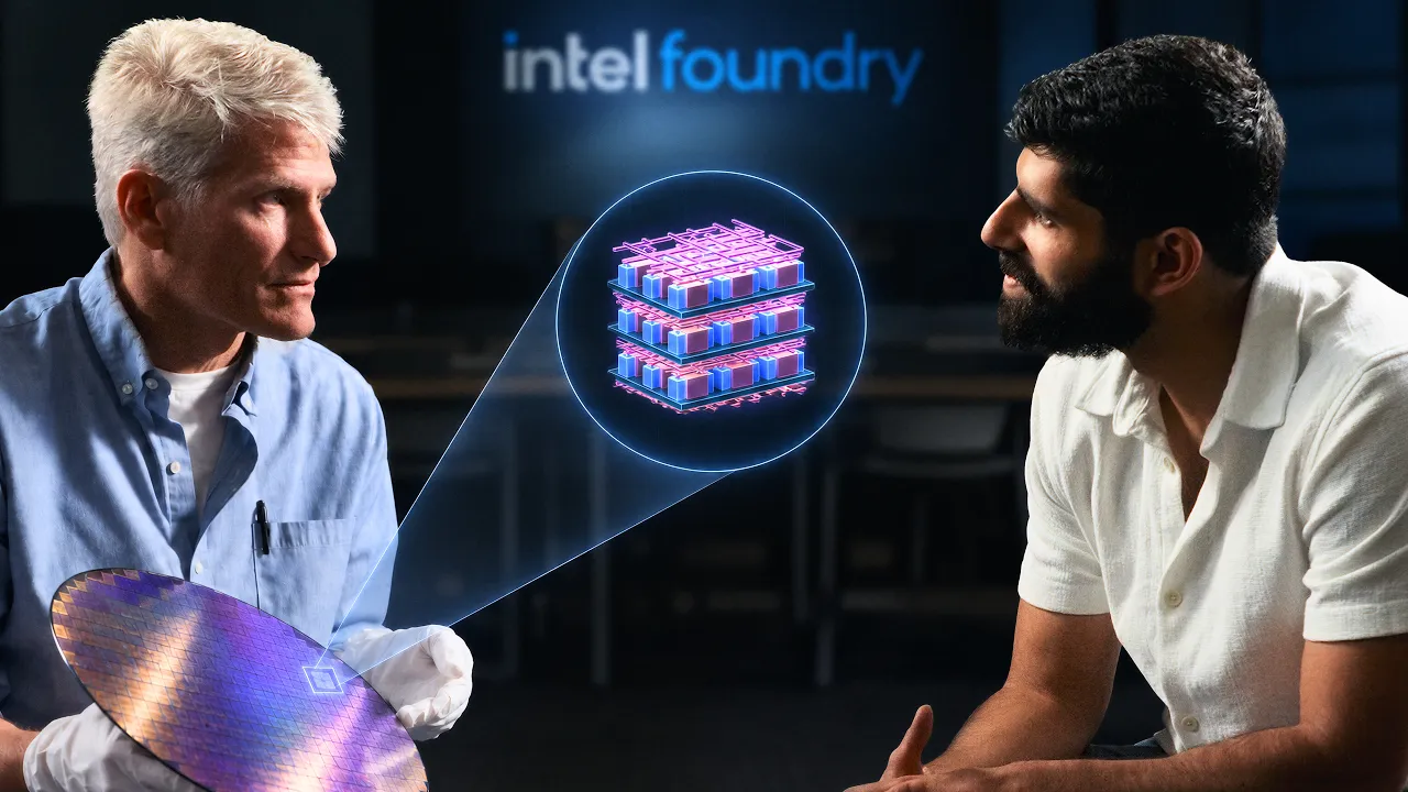
Dwarkesh Patel
Global chipmaking equipment constraints leave foundries able to only double leading-edge wafer output despite AI demand tripling yearly.
AI-assisted summary of What will computer chips look like in 2045? — original source. Check the original for full context.
Source published:
Key ideas
- Intel executives evaluate that global semiconductor tool supply chains could support doubling leading-edge wafer output, but cannot support a 10x expansion to match AI compute demand growing roughly 3x per year. (50:05)
- High-NA EUV scanners costing $350–400 million are economically viable for Intel's 14A node because backside power widens frontside wiring pitch into single-exposure range, whereas TSMC would still require double-patterning. (13:13)
- Intel is developing liner-free ruthenium interconnects to replace copper below roughly a 20nm pitch, avoiding the severe resistance and electron scattering caused by diffusion barrier liners in ultra-thin trenches. (29:30)
- Packaging interconnect pitches have dropped from 130–150 microns to 25 microns in Foveros production, with sub-10 micron hybrid bonding converging directly with fab back-end wiring to bypass upper metal layers. (45:30)
Detailed notes
## Background Published by Dwarkesh Patel on YouTube on October 22, 2026, this episode covers a two-day tour of Intel's most advanced semiconductor fabrication facilities and in-depth discussions with its technical leadership. The program explores upcoming hardware architectures like Gate-All-Around transistors, backside power, CFET, and hybrid bonding, alongside an examination of how foundries can cope with the massive demand shock brought on by AI.
## TL;DR The episode provides an inside look at the technical and economic realities of leading-edge semiconductor fabrication as the industry races toward 2045. Dwarkesh Patel tours Intel's fab and interviews key engineering executives to unpack critical architectural shifts, including the transition to RibbonFET, backside power delivery, ruthenium interconnects, and CFET monolithic 3D scaling. The discussion highlights lessons from historical execution delays, contrasting Intel's adoption of High-NA EUV with TSMC's roadmap, while examining packaging innovations like chip-to-wafer hybrid bonding. Crucially, Intel leadership addresses the structural supply crunch driven by AI compute demand, noting that while existing tool supply chains from makers like ASML might support doubling leading-edge wafer output, a 10x expansion is physically gated by equipment lead times and high capital costs.
## Atmosphere & style The presentation is intellectually rigorous, fast-paced, and deeply technical, blending journalistic curiosity with granular microelectronics engineering. Shot on location with animated visual explainers, the conversations with Intel leaders carry an air of pragmatic candor rather than corporate PR, openly confronting past failures like the 10nm delay alongside current high-stakes bets on 18A and 14A. The resulting atmosphere feels like an urgent, unvarnished debrief from the physical frontier of Moore's Law, balancing awe at atomic-scale precision with sober realism about the geopolitical and manufacturing bottlenecks constraining the AI boom.
## Bulletin - [50:05](https://www.youtube.com/watch?v=frYSOKvNiiE&t=3005s) Intel executives evaluate that global semiconductor tool supply chains could support doubling leading-edge wafer output, but cannot support a 10x expansion to match AI compute demand growing roughly 3x per year. - [13:13](https://www.youtube.com/watch?v=frYSOKvNiiE&t=793s) High-NA EUV scanners costing $350–400 million are economically viable for Intel's 14A node because backside power widens frontside wiring pitch into single-exposure range, whereas TSMC would still require double-patterning. - [29:30](https://www.youtube.com/watch?v=frYSOKvNiiE&t=1770s) Intel is developing liner-free ruthenium interconnects to replace copper below roughly a 20nm pitch, avoiding the severe resistance and electron scattering caused by diffusion barrier liners in ultra-thin trenches. - [45:30](https://www.youtube.com/watch?v=frYSOKvNiiE&t=2730s) Packaging interconnect pitches have dropped from 130–150 microns to 25 microns in Foveros production, with sub-10 micron hybrid bonding converging directly with fab back-end wiring to bypass upper metal layers.
## Key takeaways - [00:00](https://www.youtube.com/watch?v=frYSOKvNiiE&t=0s) AI compute demand growing at roughly 3x annually faces a hard physical ceiling set by upstream toolmakers like ASML, with chip demand exceeding maximum fabrication capacity by 40% to 50%. - [00:47](https://www.youtube.com/watch?v=frYSOKvNiiE&t=47s) A leading-edge node like Intel 14A requires over three years of pathfinding and roughly 2,000 discrete processing steps per wafer in the cleanroom. - [03:22](https://www.youtube.com/watch?v=frYSOKvNiiE&t=202s) Intel's costly 10nm delay stemmed from hyperscaling with DUV immersion multipatterning instead of EUV, prompting strict phase-gate metrics before nodes enter mainstream development. - [06:28](https://www.youtube.com/watch?v=frYSOKvNiiE&t=388s) The evolution from planar transistors to FinFET and Gate-All-Around (GAA) nanosheets was driven by electrostatic channel control to prevent leakage as dimensions contracted. - [13:13](https://www.youtube.com/watch?v=frYSOKvNiiE&t=793s) High-NA EUV tools double machine costs to $350–400 million, creating divergent adoption strategies between Intel and TSMC based on underlying node architectures. - [19:20](https://www.youtube.com/watch?v=frYSOKvNiiE&t=1160s) Backside power delivery decouples power delivery from signal routing by thinning wafers to tens of nanometers and flipping them, relieving frontside wire congestion. - [20:28](https://www.youtube.com/watch?v=frYSOKvNiiE&t=1228s) Complementary FET (CFET) vertically stacks NMOS and PMOS transistors to double density, but creates extreme vertical aspect-ratio etching challenges and severe thermal penalties. - [29:30](https://www.youtube.com/watch?v=frYSOKvNiiE&t=1770s) At pitches below 20 nanometers, liner-free subtractively etched ruthenium outperforms conventional copper because copper barrier liners consume too much conductive volume. - [36:43](https://www.youtube.com/watch?v=frYSOKvNiiE&t=2203s) Transitioning novel transistor architectures or 2D materials from laboratory proof-of-concept to high-volume commercial manufacturing takes roughly a full decade. - [39:45](https://www.youtube.com/watch?v=frYSOKvNiiE&t=2385s) 3D hybrid bonding eliminates solder microbumps by directly fusing atomically polished copper and dielectrics, circumventing the area-versus-perimeter edge-routing bottleneck. - [43:53](https://www.youtube.com/watch?v=frYSOKvNiiE&t=2633s) Chip-to-wafer bonding provides critical yield advantages over wafer-to-wafer bonding by allowing pre-testing and pairing only known good dies. - [53:01](https://www.youtube.com/watch?v=frYSOKvNiiE&t=3181s) Fabs have an ~80% fixed cost structure, making high utilization and percentage-point yield improvements far more economically impactful than marginal PPA advantages. - [59:11](https://www.youtube.com/watch?v=frYSOKvNiiE&t=3551s) Tooling lead times of roughly 18 months cap unexpected wafer supply expansion before 2030, meaning new fab construction cannot solve short-term shortages without additional tool output. - [01:06:26](https://www.youtube.com/watch?v=frYSOKvNiiE&t=3986s) Astronomical capital risks and machine costs doubling every 4 to 5 years enforce deep operational conservatism across incumbent foundries, entrenching decades-old design methodologies.
## Detailed walkthrough ### [00:00](https://www.youtube.com/watch?v=frYSOKvNiiE&t=0s) The AI Demand Shock and the Hardware Bottleneck
The semiconductor industry is currently navigating an unprecedented surge in demand driven by the explosion of artificial intelligence. While AI compute requirements have expanded exponentially over the last decade—roughly tripling year over year—foundries are facing a severe capacity crunch. Semiconductor executives report customer demand running anywhere from 40% to 50% above maximum fabrication limits, an imbalance of a scale never seen before in the history of chipmaking. Sustaining this level of AI progress requires chip manufacturers like Intel to drastically increase the output of leading-edge silicon, which means not only expanding raw wafer volume but also packing far greater capabilities and efficiency into every individual die.
That manufacturing ambition runs directly into physical hardware limits. Production throughput is strictly gated by the specialized fabrication equipment supplied to chipmakers, most critically the extreme ultraviolet (EUV) lithography systems manufactured exclusively by Dutch supplier ASML. Without these massive, multimillion-dollar machines installed and running on the factory floor, advancing production is impossible. To understand how the semiconductor ecosystem plans to navigate this supply-demand bottleneck and what future silicon architectures will look like, Dwarkesh Patel toured Intel’s premier fabrication facilities and met with the company's technical leadership.
[00:47](https://www.youtube.com/watch?v=frYSOKvNiiE&t=47s) Bringing Up a Process Node: The 2,000 Steps of 14A
Dwarkesh sits down with Chris Auth, who oversees development for all processes currently heading toward high-volume manufacturing at Intel. Dwarkesh asks how a future process node—such as Intel 14A, slated for commercial release two to three years out—is systematically developed, tested, and fine-tuned over time. Auth explains that by the time a node reaches this phase, it has already undergone more than three years of intensive pathfinding and pre-work. At the current stage, Intel engineers are locking down the final process window, finalizing the exact toolsets required across the fab, and optimizing each individual operational step.
Fabricating a cutting-edge wafer requires approximately 2,000 distinct processing steps inside the cleanroom. Every single one of these steps must be engineered for extreme repeatability so the fab can reliably process thousands of wafers every week with predictable yields. Yield improvement does not happen by chance; it relies on relentless defect tracking across two core avenues:
- **Inline Metrology:** Automated inspection tools inspect wafers directly during the manufacturing process, flagging particulate contamination and physical anomalies as they appear layer by layer. - **End-of-Line Electrical Testing and Sorting:** Finished wafers undergo electrical sorting to identify circuit failures. When a die fails, failure analysis teams excise microscopic cross-sections of the defect using transmission electron microscopy (TEM) in the lab.
By analyzing these physical cross-sections, engineers identify the exact vertical layers where a short or void occurred. They trace that location back to the specific manufacturing station in the 2,000-step flow and correlate it with inline inspection data to eliminate the root cause. As Auth emphasizes, managing this complexity requires discipline: “What we’ve learned is that you don’t want to do too much innovation in one node, because the more innovation that you do, the more complex it becomes.”
[03:22](https://www.youtube.com/watch?v=frYSOKvNiiE&t=202s) The Lessons of 10nm: Hyperscaling and Phase Gates
Intel's conservative philosophy around node complexity stems directly from the painful setbacks it suffered on its 10-nanometer process node. Historically, Intel drove the two-year cadence of Moore’s Law, but the 10nm process—originally scheduled for high-volume deployment in 2016—slipped until late 2018, causing products to fall nearly four years behind schedule. When Intel announced the delays, its stock plunged more than 15% in a single trading session, while its chief rival, Taiwan Semiconductor Manufacturing Company (TSMC), rallied 13%.
Auth explains that 10nm was characterized by an overly ambitious push known internally as "hyperscaling." Intel attempted to shrink transistor features far faster than the historical rate while relying on existing deep ultraviolet (DUV) immersion lithography tools because next-generation equipment was not ready. To achieve that aggressive scaling without new tools, engineers devised convoluted multipatterning schemes that placed an unsustainable burden on process development and engineering teams. Although 10nm eventually matured into a high-yielding, high-performing, and cost-effective node, the delay cost Intel its manufacturing lead.
The biggest tactical error of that era was concluding that extreme ultraviolet (EUV) lithography was not ready. EUV uses light with a 13.5-nanometer wavelength—roughly 14 times shorter than the 193-nanometer light emitted by previous DUV immersion scanners—allowing fine features to be printed in a single exposure rather than multiple passes. While Intel opted to bypass EUV for 10nm, TSMC leaned aggressively into the technology, entering commercial high-volume EUV manufacturing in 2019 and scaling it widely across its 5nm node in 2020. Intel did not field its first EUV-based production node until 2023, handing TSMC a four-year head start in tool calibration and operational expertise.
To ensure such delays never repeat, Intel overhauled its operational management by instituting rigorous "phase gate" criteria: - Research and pathfinding initiatives can only transition into mainstream process development if they satisfy predefined maturity metrics for defect levels, yield predictability, and baseline electrical performance. - Any exploratory technology—whether 2D materials, complementary FETs (CFET), or novel metals like ruthenium—that fails to meet its phase-gate milestones is immediately pushed to a later node rather than allowed to compromise the delivery date. - As Auth summarizes the core lesson: “Having that predictable schedule is a key piece. You’ve got to figure out how much innovation you can put in in order to meet the customer’s requirements in the timeline that they need it.”
[06:28](https://www.youtube.com/watch?v=frYSOKvNiiE&t=388s) From Planar to Gate-All-Around: The Architecture of Modern Transistors
To understand modern process engineering, one must look at how transistor structures have evolved from two-dimensional surfaces into complex three-dimensional architectures. Every field-effect transistor functions fundamentally as an electronic switch. Applying a positive electrical voltage to the gate pulls negatively charged electrons through the underlying silicon, gathering them just beneath a thin insulating barrier to form a conductive "channel" connecting the source to the drain. Removing the voltage causes the electrons to disperse, closing the channel and turning the switch off.
As transistors shrank down to nanoscale dimensions, the physical distance separating the source from the drain became exceedingly narrow. Consequently, the gate lost electrostatic control over the channel, allowing unwanted leakage current to slip through even when the switch was nominally off. To restore control and suppress parasitic leakage, chip designers had to increase the surface area between the gate and the channel:
```mermaid flowchart LR accTitle: Evolution of Transistor Gate Architectures accDescr: Diagram tracking transistor architectures from 2D Planar to 3D FinFET and Gate-All-Around nanosheets.
subgraph Planar["Planar Transistor (1960)"] direction TB P1["Flat Silicon Channel"] --> P2["Gate Touches Top Surface Only"] P2 --> P3["Vulnerable to Short-Channel Leakage"] end
subgraph FinFET["FinFET (Lab: 1989 / HVM: 2011)"] direction TB F1["Vertical Silicon Fin Channel"] --> F2["Gate Wraps Around 3 Sides"] F2 --> F3["Improved Electrostatic Control"] end
subgraph GAA["Gate-All-Around / RibbonFET"] direction TB G1["Suspended Silicon Nanosheets"] --> G2["Gate Wraps All 4 Sides"] G2 --> G3["Maximum Electrostatic Drive & Density"] end
Planar -->|"Scale limits reached"| FinFET FinFET -->|"Fin pitch limits reached"| GAA ```
- **Planar Transistor (1960):** The classical metal-oxide-semiconductor (MOS) architecture where the gate sits flat on top of the silicon channel, exerting electrostatic control strictly from a single side. - **FinFET (Commercialized by Intel in 2011):** The silicon channel is extruded upward into a slender, three-dimensional vertical fin. The conductive gate drapes over the fin, wrapping around three sides (top, left, and right) to clamp down on sub-threshold leakage. - **Gate-All-Around (GAA) / RibbonFET:** The channel is sliced horizontally into a vertical stack of discrete, suspended silicon ribbons (nanosheets). The gate material wraps completely around all four sides of every individual ribbon, maximizing electrostatic drive current while suppressing off-state leakage.
Manufacturing GAA ribbons requires an intricate, multistage chemical sequence. In the fab, alternating layers of silicon and a temporary sacrificial material (silicon germanium) are grown epitaxially to create a layered sandwich. Because permanent high-dielectric (high-k) gate materials and metal gates cannot withstand the downstream high-temperature processing steps—which involve annealing the wafer at roughly 1,000 degrees Celsius—a temporary placeholder gate holds the structure in place. Once high-temperature processing is complete, the sacrificial silicon-germanium layers are selectively etched away, leaving the silicon ribbons hanging freely in open space. Next, an ultra-thin conformal layer of high-k insulating dielectric is deposited around every exposed ribbon to enhance electrostatic coupling, followed by the deposition of the final metal gate.
Though both FinFET (demonstrated in 1989) and Gate-All-Around (demonstrated in 1988) were conceived in research laboratories around the same time, their arrival in commercial high-volume manufacturing (HVM) occurred more than a decade apart. Intel introduced FinFET in 2011 at the 22nm node, whereas the first commercial GAA transistors were not shipped until Samsung deployed them in 2022. Asked why GAA took over three decades to reach production, Auth notes that having an architectural concept in the 1990s was only the beginning. The industry still had to invent, qualify, and sequence interim scaling solutions—such as strained silicon, high-k metal gate (HKMG), and FinFETs—before the massive tooling and material hurdles of GAA could be justified in high-volume production.
[10:17](https://www.youtube.com/watch?v=frYSOKvNiiE&t=617s) Transistor Scaling: From Dennard Scaling to the “Golden Age of Innovation”
Addressing why major architectural shifts take so long to introduce, an Intel engineering leader explains that foundries deliberately avoid taking on risky, complex challenges before they have to. As long as alternative levers can deliver the required performance gains, engineers pursue those first. Intel progressed along this incremental path by implementing strained silicon, high-κ metal gate (HKMG), and FinFETs before confronting the necessity of gate-all-around (GAA) architectures. GAA represents the ultimate transistor structure, but adopting it forces engineers to reinvent how to integrate past breakthroughs—such as high-κ metal gates—into the new geometry.
This level of innovation takes time because it frequently depends on materials that have never been used in semiconductor fabs and brand-new machinery that tool vendors must invent from scratch. Intel engineers must approach vendors specifying precise requirements: a machine capable of a novel deposition technique, a chemistry/gas capable of laying down a specific layer, or a specialized heating chuck with unique thermal characteristics. The R&D cycle is intensely iterative; teams produce test GAA transistors, discover failures, reassess their initial hypotheses, and test modified structures.
This stands in stark contrast to the R&D model of the 1980s and 1990s. In that era, the industry rode classical Dennard scaling and standard optical lithography. The recipe was predictable: scale dimensions downward, and transistors naturally became faster, more reliable, and more energy-efficient without changing the fundamental process flow. Once Dennard scaling broke down in the 2000s, simply shrinking features ceased to work. Reflecting on this turning point, the speaker notes:
> “Before, it was, ‘Try to not change anything.’ Now it’s, ‘Take the sledgehammer and start tearing the thing up and come up with some new idea.’”
Rather than lamenting the demise of Dennard scaling, he describes the subsequent period as an exciting golden age for a self-described "transistor junkie." The playbook opened up completely to structural inventions and exotic materials:
- The variety of materials deployed in advanced fabs today is roughly 10× higher than in the 1990s. - Modern fabrication relies on techniques like atomic layer deposition (ALD), which deposits films and controls surfaces literally atom by atom. - The cadence shifted from maintaining a fixed process flow to introducing major structural innovations at each node: strained silicon, HKMG, FinFETs, gate-all-around nanosheets, and backside power delivery.
```mermaid flowchart LR accTitle: Evolution of Transistor Scaling Paradigms accDescr: Shows the progression from Dennard scaling to the modern era of structural innovations and new materials.
subgraph Classical["1980s–1990s: Dennard Era"] A["Planar Transistors"] --> B["Shrink Dimensions"] B --> C["Same Process Flow"] end
subgraph Modern["2000s–Present: Structural Innovation"] D["Strained Silicon"] --> E["High-κ Metal Gate"] E --> F["FinFETs"] F --> G["Gate-All-Around & Backside Power"] end
C -->|"Dennard Scaling Breaks"| D ```
---
[13:13](https://www.youtube.com/watch?v=frYSOKvNiiE&t=793s) High-NA EUV: Why It Makes Sense for Intel but Not TSMC
For its upcoming 14A node, Intel is adopting High Numerical Aperture Extreme Ultraviolet (High-NA EUV) lithography. Both standard EUV and High-NA EUV utilize light at a 13.5 nm wavelength, but High-NA redesigns the optical train to project light through a larger lens opening. Numerical aperture measures how wide a cone of light the mirror optics can focus onto the wafer surface; a wider cone produces a smaller focused spot, allowing finer features to be printed. While standard EUV systems feature an NA of 0.33, High-NA systems increase the aperture to 0.55. This enables High-NA tools to print patterns roughly 1.7× smaller in a single exposure pass.
When transistor or wire dimensions shrink below a lithography tool's single-exposure resolution limit, chipmakers must resort to multi-patterning—splitting the design layout across two, three, or four separate masks and passes. Every additional pass consumes throughput on lithography equipment costing approximately $200 million per machine while compounding defect opportunities and edge-placement errors. Although High-NA machines cost roughly double an existing EUV tool (approaching $350–400 million), they eliminate the need for multi-patterning passes. The economic viability of High-NA boils down to whether the cycle time saved and defect reduction outweigh the machine's exorbitant capital cost.
TSMC has publicly taken the position that High-NA does not make economic sense for them in the near term, whereas Intel is adopting it on 14A. This divergence stems directly from their architectural choices around backside power delivery:
> “High-NA’s a good example of where, because of the architecture of our technology versus TSMC’s, we make different conclusions off of the same tool set.”
```mermaid flowchart TD accTitle: Comparison of Backside Power vs Standard Frontside Routing for High-NA Lithography accDescr: Illustrates how backside power relieves pitch requirements to allow single-pass High-NA printing.
subgraph IntelPath["Intel 14A Architecture"] direction TB A1["Power Lines Moved to Backside"] --> B1["Relieved Pitch on Frontside Signal Wires"] B1 --> C1["Direct Single-Pass High-NA EUV Printing"] C1 --> D1["Cost & Defect Reduction"] end
subgraph TSMCPath["Conventional Architecture"] direction TB A2["Signal & Thick Power Packed on Front"] --> B2["Extremely Tight Pitches Required"] B2 --> C2["Tighter Than Single High-NA Pass Pitch"] C2 --> D2["Must Use Multi-Patterning EUV; High-NA ROI Falls"] end ```
In a traditional chip, thick, low-resistance power distribution rails and thin signal interconnects must share the upper metallization stack above the silicon substrate. Because signal lines must be spaced carefully to prevent cross-talk and capacitive coupling, crowding both power and signal on the front creates an interconnect bottleneck. Intel’s architecture separates the two networks: power rails are routed underneath the active silicon from the back of the wafer, freeing up frontside routing space.
Because Intel uses backside power, frontside interconnect pitches do not need to be forced down to extreme dimensions, falling directly into the sweet spot that can be resolved in a single High-NA exposure. TSMC, relying on conventional frontside power delivery for earlier generations, must pack lines so tightly that even a single High-NA pass cannot resolve them without multi-patterning. For TSMC, adopting High-NA would still require double-patterning, invalidating the machine's economic justification. On 14A, Intel offers High-NA as an optional customer configuration, weighing specific project value against the added process complexity.
---
[16:13](https://www.youtube.com/watch?v=frYSOKvNiiE&t=973s) The Foundry Learning Curve: Developing Customer-Ready PDKs
Transitioning from an Integrated Device Manufacturer (IDM) that fabricates internal designs into a merchant foundry serving external customers requires Intel to undergo a steep learning curve. Historically, Intel’s design and manufacturing groups collaborated through close internal feedback; fab engineers shared raw transistor data with internal architecture teams without requiring a rigid, industry-standard Process Design Kit (PDK). A foundry, however, must provide external fabless clients with a comprehensive PDK—a formalized rulebook detailing design rules, device models, schematic-driven layout constraints, and design-for-manufacturability parameters.
Public reports surfaced regarding early delays and maturity issues with the PDK on the 18A node, where external customers found initial documentation and rule decks difficult to work with. Intel acknowledges that 18A originally began without the refined PDK infrastructure standard foundries offer. Foundry competitors took decades to mature their external interfacing, and Intel has had to rapidly incorporate customer feedback regarding rule completeness, verification accuracy, and release readiness.
Intel measures PDK development against standardized maturity benchmarks (progressing through PDK 0.5, PDK 0.9, to general production 1.0). The lessons learned from the 18A bring-up have been folded into 14A, which is architected to provide mature, high-quality PDKs from the start of customer engagement. Historically, internal-only manufacturing limited Intel to its own product volumes, whereas TSMC’s open foundry model granted it exposure to diverse customer workloads, vastly higher total wafer volumes, rapid operational learning cycles, and relentless schedule discipline.
---
[19:20](https://www.youtube.com/watch?v=frYSOKvNiiE&t=1160s) The Tech Tree: Historical Inevitability vs. Radical Shifts
When asked whether semiconductor history could have diverged along an entirely different "tech tree"—perhaps bypassing gate-all-around entirely—the Intel leader reflects on the inevitability of specific physics-driven breakthroughs versus radical engineering bets. Transistor channel control follows fundamental electrostatic laws: as channel lengths scale down to the nanometer regime, the gate electrode must enclose the channel on more sides to maintain gate control and suppress sub-threshold leakage currents. The evolution from planar (1 side) to FinFET (3 sides) and ultimately to gate-all-around (4 sides) was an electrostatic imperative that researchers anticipated as far back as the 1990s.
In contrast, other modern techniques were far from obvious:
> “Backside power, that one’s pretty out there. Even in the ’90s, the idea that you’re going to strip off the entire silicon substrate and put lines on the backside, that one is probably something that’s a little bit out there.”
The realization of backside power requires grinding away almost the entire bulk silicon wafer down to a layer only tens of nanometers thick, flipping the wafer, bonding it to a carrier substrate, and constructing a multi-layer metallization grid on the reverse side with lithographic alignment through the wafer.
Regarding wiring materials, copper remains the dominant standard for bulk on-chip wiring due to its exceptional electrical conductivity and electromigration resistance. However, copper hits a physical limit at the lowest metallization layers: when wire dimensions become smaller than the mean free path of an electron in copper, electron scattering off sidewall barriers and grain boundaries causes resistance to skyrocket. Consequently, while copper will remain standard for upper, wider interconnect layers, Intel confirms that replacing copper with alternative metals (such as ruthenium) is becoming inevitable for the absolute tightest pitches.
[20:28](https://www.youtube.com/watch?v=frYSOKvNiiE&t=1228s) 3D Stacking, CFET, and the Thermal Bottleneck
Transitioning to gate-all-around (GAA) architectures and backside power delivery fundamentally shifts the paradigm of chip construction. Historically, chips were built strictly from the bottom up on top of a single substrate. Under this new regime, a transistor essentially floats suspended inside the interconnect layers, prompting architects to question why they cannot simply alternate layers of transistors and wiring into fully integrated 3D monolithic structures, rather than just stacking discrete chips together. While 3D architectures are already mature in memory technologies like NAND and are actively being pursued for DRAM, logic presents a much steeper challenge. Industry roadmaps are often artificially constrained by short planning cycles of roughly four years, making speculative architectures for 2045 seem impossibly distant, even though incremental four-year leaps eventually make exotic structures achievable. As an Intel technologist points out regarding long-term visibility: “We limit ourselves by what we see as possible in the next four years.”
```mermaid flowchart TD accTitle: Transistor Evolution from Planar to 3D Stacking accDescr: Progression showing how planar side-by-side transistors evolve into GAA, CFET, and integrated 3D monolithic logic.
subgraph Planar["Traditional Architecture"] direction LR P1["Substrate Base"] --> P2["Side-by-Side N-type & P-type"] P2 --> P3["Standard Top Interconnect"] end
subgraph Modern["GAA & Backside Power"] direction LR G1["Backside Interconnect (Power)"] --> G2["Floating GAA Transistors"] G2 --> G3["Frontside Interconnect (Signal)"] end
subgraph Future["Monolithic 3D & CFET"] direction LR C1["Stacked CFET (N-over-P)"] --> C2["Alternating Interconnects"] C2 --> C3["Multi-layer 3D Logic"] end
Planar --> Modern --> Future ```
The immediate vertical leap begins with the transistors themselves through Complementary Field-Effect Transistors (CFET). Standard circuits require pairing complementary n-type and p-type transistors, which operate identically but with inverted electrical charges. Currently, chipmakers fabricate these pairs side by side. CFET stacks the n-type and p-type directly atop one another, doubling transistor density within the exact same footprint. However, building upward in logic introduces severe thermal penalties that memory stacks like High Bandwidth Memory (HBM) and 3D NAND do not experience to the same degree, because active logic consumes vastly more power.
Addressing whether heat dissipation represents the ultimate long-term ceiling for computing, Intel leadership notes that computing limits have always boiled down to three fundamental, interconnected pillars: switching frequency (how fast the device toggles), power efficiency (how much energy each switch consumes), and heat dissipation (how efficiently generated thermal energy is removed). While these three limiters have been debated in literature for over two decades, system-level simulation and analysis tools specifically tailored to 3D logic thermal dissipation remain in their infancy.
- CFET stacks n-type and p-type transistors vertically to achieve up to a 2x density increase over side-by-side placement. - Three fundamental physics limits govern compute scaling: device switching frequency, power efficiency per switch, and thermal dissipation. - Long-range process technology development typically maintains high visibility only for about a four-year horizon at any given time.
[23:45](https://www.youtube.com/watch?v=frYSOKvNiiE&t=1425s) Inside Intel's "Hot Topics" Meeting and Risk Culture
Engineering resources, tool time, and physical test wafers are strictly finite, meaning the hundreds of micro-experiments required to bring up advanced process nodes like Intel 18A and 18A-P must be ruthlessly triaged. That prioritization happens inside Intel’s high-stakes "Hot Topics" meetings, led by senior integration figures like Kevin Fischer. In these sessions, process and integration engineers pitch experiments aimed at raising yields and boosting drive currents, while leadership decides which data is missing, which experiments proceed, and how to accelerate cycle times. Fischer emphasizes that bringing up a leading-edge node demands an aggressive operational pace, where waiting for absolute certainty is fatal: “One thing you learn in this industry is that you will never have a complete data set.”
Fischer acknowledges that his assertive posture in these meetings can make him seem demanding, but he views it as an indispensable driver of corporate urgency. Frontline research engineers often operate within narrow technical silos; when they encounter a cross-functional denial or an organizational roadblock, their instinct is often to stop and accept the barrier. Leadership must intervene to force calculated risks directly onto the factory floor, weighing technical unknowns against the immediate risk to production schedules and commercial revenue. As Kevin Fischer frames the urgency required to protect node delivery: “If you want to wait for a complete data set, you’ve waited too long. It’s already too late.”
[26:39](https://www.youtube.com/watch?v=frYSOKvNiiE&t=1599s) Tackling Epi Nodules and the "Hot Box" Priority System
One concrete defect discussed in the Hot Topics meeting involves epitaxial growth, commonly referred to as "epi." In chip manufacturing, epitaxy involves flowing heated gases over a wafer surface so precursor atoms deposit precisely along the underlying crystalline lattice, using that base structure as an atomic template. Intel utilizes epitaxy to grow the raised source and drain crystals flanking the gate channel. During deposition, abnormal, hyper-accelerated crystalline growths—resembling microscopic tumors—can erupt on the wafer. These epi nodules bridge unintended gaps, causing direct shorts between adjacent source/drain regions and killing functional yield.
Resolving node-threatening defects like nodules requires running multiple parallel tracks: developing specialized post-growth cleaning flushes to strip the nodules away after they nucleate, while simultaneously troubleshooting the deposition chamber kinetics to eliminate the root contamination source. To accelerate these pivotal trials, the fab operates a tiered priority system known as "hot boxes." The most critical classification, HotBox 1, grants a wafer lot absolute right-of-way across every tool in the facility, clearing all standard queue times. Because halting normal production lots to clear tools for a single experiment significantly degrades overall factory efficiency and tool utilization, manufacturing managers treat HotBox 1 sparingly, comparing it to an open diamond carpool lane where all normal highway traffic is cleared aside so one car can race through unimpeded.
- Epitaxy (epi) uses gas-phase precursors to continue the underlying substrate's single-crystal lattice structure to form transistor source and drain terminals. - Epi nodules act as localized crystalline shorts between adjacent terminals, rendering the underlying transistor circuitry completely inoperable. - Intel factories use a graded "hot box" priority hierarchy; HotBox 1 lots bypass all tool queues but introduce throughput drag across the fab line. - Parallel defect mitigation requires pursuing curative cleans alongside upstream root-cause chamber fixes simultaneously.
*(Dwarkesh highlights sponsor Jane Street, noting how their engineers repurposed Intel's hardware-level Processor Trace feature—which records fine-grained instruction streams and function calls—to build an internal diagnostic tool called magic-trace for pinpointing microsecond-level network latency anomalies in live trading systems.)*
[29:31](https://www.youtube.com/watch?v=frYSOKvNiiE&t=1771s) Replacing Copper with Ruthenium Interconnects
Beyond the active transistor level lies the interconnect stack: more than a dozen intricate layers of metal wiring responsible for routing signals and power across billions of transistors. For decades, copper has served as the industry-standard metal for these lines. However, as wire pitches drop down to extreme dimensions, copper exhibits steep increases in electrical resistance. In Intel’s research labs, Jack Kavalieros and research teams are actively investigating alternative conductive materials, focusing heavily on elemental ruthenium as a successor for tight-pitch wiring layers.
```mermaid flowchart LR accTitle: Copper vs. Ruthenium Interconnect Cross-Section accDescr: Comparison showing how copper requires a resistive liner that chokes scaled wires, whereas etchable ruthenium eliminates the liner entirely.
subgraph CopperWire["Scaled Copper Interconnect"] direction TB C_Liner["Resistive Diffusion Liner / Glue Layer"] C_Core["Constricted Copper Conductor Core"] C_Liner --- C_Core end
subgraph RutheniumWire["Scaled Ruthenium Interconnect"] direction TB R_Core["Full-Volume Ruthenium Conductor (Directly Etched / Liner-Free)"] end
CopperWire -.->|"Pitches below ~20nm"| RutheniumWire ```
While bulk ruthenium inherently possesses higher electrical resistivity than bulk copper, it behaves far better at extremely small geometries. Copper wiring cannot be laid down directly against dielectric insulating material; it requires a protective barrier or "liner"—an adhesive transition layer that prevents copper atoms from migrating into the adjacent insulator and ensures proper adhesion. At tightly scaled pitches, this resistive liner consumes an increasingly large fraction of the trench volume, leaving only a tiny conduit for actual copper conduction. Ruthenium, by contrast, can be directly patterned and etched cleanly without requiring a diffusion liner, maximizing the active cross-sectional conducting area. At pitch dimensions below roughly 20 nanometers (where approximately half the pitch is the metal line and half is the insulating dielectric), ruthenium crosses over to provide superior net conductivity compared to lined copper.
- Modern logic chips contain more than a dozen stacked metallization layers forming the interconnect network. - Conventional copper lines require resistive diffusion barrier liners to guarantee mechanical adhesion and prevent atomic drift. - Ruthenium can be subtractively etched without an adhesive liner, eliminating the volume penalty imposed by conventional barrier layers. - The resistivity crossover threshold where liner-free ruthenium outperforms lined copper occurs around a 20-nanometer interconnect pitch. - As Jack Kavalieros explains regarding the geometry trade-off: “Now you scale those very fine dimensions, and if you can trade off that resistive liner with no liner, ruthenium starts to win.”
[31:05](https://www.youtube.com/watch?v=frYSOKvNiiE&t=1865s) The Materials Tradeoff: Copper, Cobalt, and Ruthenium
The interconnect stack consists of interlocking copper lines routed to form electrical pathways throughout the die. Historically, depositing copper has always required an underlying barrier or liner layer. At older process dimensions, that liner occupied a significant share of the total cross-sectional area, choking off the conduction path. However, as fabrication teams scaled and thinned down the liner over time, copper re-emerged as the strongest contender for the interconnect layers.
```mermaid flowchart LR accTitle: Evolution of Interconnect Metal Choices accDescr: Progression showing early copper with thick liners moving to cobalt, then back to copper with thin liners, and toward ruthenium.
subgraph Past["Past Nodes"] A["Copper + Thick Liner<br/>(Liner limits conduction)"] B["Cobalt<br/>(Selected for 10nm)"] end
subgraph Present["Current Nodes"] C["Copper + Thinned Liner<br/>(Regains dominance)"] end
subgraph Future["Future Nodes"] D["Ruthenium<br/>(Potential next-gen metal)"] end
A -->|"10nm transition"| B B -->|"Liner scaling"| C C -->|"Atomic limits"| D ```
When Dwarkesh Patel asks how engineers determine whether a material transition is ready for high-volume manufacturing—pointing out the difficulties Intel faced when moving from copper to cobalt at the 10nm node—the response highlights the friction between isolated material capability and holistic integration. Decisions must be made under strict delivery deadlines, evaluating vendor toolsets, scalability, and how materials interface with neighboring transistor structures. As the Intel engineer explains:
> “At the time we made a decision for cobalt, it was the forerunner. The results were stronger at the time. But as we work with our ecosystem externally, the vendor ecosystem that provides these materials and the tools that we integrate them with, we find solutions down the road that may bring copper back in line as being the stronger of the two.”
- Integrating replacement materials depends on tool readiness across the entire supplier ecosystem, not just standalone electrical performance in a test vehicle. - For each upcoming node, Intel continuously evaluates multiple metallization alternatives as the delivery deadline approaches. - While cobalt took precedence at 10nm, copper returned once liner technology improved, and ruthenium stands as the potential successor for future fine-pitch layers.
---
[32:41](https://www.youtube.com/watch?v=frYSOKvNiiE&t=1961s) CFET and Vertical Scaling Challenges
Complementary FET (CFET) represents the eventual shift toward vertically stacking transistors on top of one another, pursued by Intel, its direct competitors, and academic research labs alike. Traditional planar scaling forced NMOS and PMOS devices into increasingly compressed side-by-side lateral footprints. CFET relaxes lateral footprint constraints by putting one device directly over the other, but it introduces a severe vertical wiring problem. Connections that previously ran laterally across the top or bottom surface must now plunge vertically between the stacked channels.
The primary manufacturing bottleneck centers on high-aspect-ratio processing. Etching deep, ultra-narrow vertical trenches between the devices pushes physical limits. Once etched, these deep cavities must be completely filled with metal and dielectric layers without leaving voids or trapped air pockets, which degrade structural and electrical integrity.
- CFET moves NMOS and PMOS from adjacent lateral positions to a stacked 3D arrangement. - Moving connections vertically dramatically increases the aspect ratio of required vias and trenches. - Filling these high-aspect-ratio voids without creating air gaps remains a major obstacle for fabrication tool vendors.
---
[34:06](https://www.youtube.com/watch?v=frYSOKvNiiE&t=2046s) Prototyping Architectures via Short-Loop Test Vehicles
Full high-volume semiconductor processes require thousands of individual processing steps and run for a month or longer per wafer. To avoid paralyzing turnaround times when developing complex architectures like CFET, Intel relies on "short-loop" test vehicles. These targeted test vehicles isolate specific unit cells—such as individual diodes, isolated capacitors, or simplified single-nanoribbon pairs—allowing engineers to rapidly gather chemical and electrical parameters before combining them into full-flow prototypes.
```mermaid flowchart TD accTitle: Short-Loop Development Flow for CFET accDescr: Step-by-step evolution from basic electrical components to full multi-ribbon CFET architectures.
subgraph UnitLevel["Unit Cell Evaluation"] U1["Isolated Components<br/>(Diodes, Capacitors)"] U2["Single-Ribbon Stack<br/>(1 NMOS wire over 1 PMOS wire)"] end
subgraph Integration["Vehicle Scaling"] I1["High-Aspect-Ratio Metallization"] I2["EUV / E-Beam Patterning Verification"] end
subgraph Target["Full High-Volume Manufacturing"] P1["Full CFET Stack<br/>(4 Ribbons over 4 Ribbons)"] end
U1 --> U2 U2 --> I1 I1 --> I2 I2 --> P1 ```
Rather than jumping directly to an eight-ribbon stack (such as four NMOS ribbons over four PMOS ribbons), early functional CFET prototypes use a single-wire architecture (one NMOS wire over one PMOS wire). This dramatically reduces the vertical aspect ratio while preserving the ability to evaluate vertical gate control, inter-device spacing, and cross-tier contact routing.
- Full wafer manufacturing runs require thousands of steps and over a month of processing time, making quick iteration impossible on standard production flows. - Short-loop vehicles validate unit operations, isolating whether a single layer, junction, or dielectric meets baseline specifications. - Current lab prototypes utilize EUV lithography and electron-beam (E-beam) patterning to test geometries that match the exact physical dimensions targeted for eventual high-volume production. - R&D lines are actively experimenting with 2D materials, such as transition metal dichalcogenides (TMDs), which form single-atom-thick monolayers for ultra-scaled channel conduction.
---
[36:43](https://www.youtube.com/watch?v=frYSOKvNiiE&t=2203s) The Decade-Long Path from Lab Prototype to High-Volume Production
Dwarkesh questions why, if working CFET devices with production-scale feature sizes already function inside Intel's development labs, it still takes approximately a decade for those innovations to reach consumer electronics. The Intel engineer contrasts the adoption of novel materials with that of novel 3D architectures. While materials present basic chemical compatibility hurdles, full architectural shifts compound geometric and manufacturing stress across every step of the fab.
A lab prototype with a single ribbon stacked over another ribbon proves physical feasibility, but it does not deliver an immediate commercial performance gain over mature side-by-side nanoribbon (gate-all-around) designs. Extracting superior performance requires scaling to multi-ribbon tiers, refining contact resistances, perfecting selective deposition, and ensuring that hundreds of downstream thermal and chemical steps do not degrade delicate underlying layers. As the engineer details:
> “There’s a thousand different steps that all have to come together in a very unique way to make the performance compatible or actually supersede the prior technology.”
When screening experimental candidates like 2D materials, failure often strikes at basic mechanical or thermal interfaces. An engineer can successfully deposit a single-atom monolayer and verify its electrical properties, only to discover that the subsequent metallization layer exhibits zero physical adhesion. In other cases, capping layers fail to form a true hermetic seal; subsequent chemical washes or reactive process gases seep past the cap, altering the material's internal lattice structure and forcing the team to scrap the concept.
- A proof-of-concept device operating in a laboratory does not automatically match the yield, reliability, or drive current of the mature generation it seeks to replace. - Simple material failures include poor surface adhesion, where overlying contacts physically peel off the active channel. - Gas permeability issues can ruin candidate materials when downstream processing gases penetrate non-hermetic barrier caps and destroy device stability.
---
[39:45](https://www.youtube.com/watch?v=frYSOKvNiiE&t=2385s) The Interconnect Bottleneck and the Rise of Hybrid Bonding
While stacking individual transistors vertically remains confined to advanced R&D, stacking entire silicon dies is already deployed in volume manufacturing to bypass data movement bottlenecks. Modern AI processors—such as Nvidia’s Blackwell platform, which combines two monolithic processor dies bordered by eight high-bandwidth memory (HBM) stacks—are governed primarily by data-transfer rates rather than raw compute cycles.
```mermaid flowchart TD accTitle: Evolution of Packaging Technologies accDescr: Transition from side-by-side planar chip wiring to 2.5D interposers and direct 3D hybrid bonding.
subgraph Standard["2D Packaging"] A["Side-by-side dies<br/>Perimeter edge wiring"] end
subgraph Interposer["2.5D Packaging"] B["Silicon Interposer<br/>High-density surface routing"] end
subgraph Direct3D["3D Hybrid Bonding"] C["Direct Cu-to-Cu & Oxide-to-Oxide Fusion<br/>Eliminates solder bumps entirely"] end
A -->|"Overcoming perimeter limits"| B B -->|"Eliminating bump resistance"| C ```
When two planar chips communicate along adjacent edges, doubling their dimensions quadruples their internal circuit area while merely doubling the available edge perimeter for I/O routing. This classic area-versus-perimeter scaling penalty forces data traffic to congest at the perimeter. The semiconductor industry addresses this by evolving through three distinct packaging eras:
| Packaging Generation | Mechanical Structure | Electrical Interface | Key Limitation | |:--- |:--- |:--- |:--- | | **2D Packaging** | Chips placed side-by-side on substrate | Edge-to-edge wire bonding or traces | Strictly limited by perimeter length | | **2.5D Packaging** | Multiple dies placed on a shared silicon interposer | Through-silicon traces and microbumps | Solder bump pitch and parasitic capacitance | | **3D Hybrid Bonding** | Direct vertical fusion of stacked silicon dies | Direct copper-to-copper & dielectric fusion | Extreme cleanliness and alignment tolerances |
Hybrid bonding eliminates traditional solder microbumps entirely. Because microbumps are physically bulky, introduce parasitic resistance, and demand minimum pitch clearances, they cap interconnect density. In hybrid bonding, copper pads and surrounding dielectric surfaces are polished atomically flat, carefully aligned, brought into contact, and heated. The copper expands thermally to form a seamless electrical connection while the dielectric fuses simultaneously, yielding a dramatic leap in interconnect density.
- In large-scale AI workloads, system throughput is predominantly throttled by chip-to-chip bandwidth rather than raw compute capabilities. - The area-versus-perimeter scaling bottleneck means computational capacity expands quadratically with chip size while edge-to-edge communication channels expand only linearly. - Hybrid bonding achieves unprecedented interconnect density by bypassing solder bumps, pushing copper pads into direct, seamless fusion alongside adjacent dielectric bonding layers.
[42:12](https://www.youtube.com/watch?v=frYSOKvNiiE&t=2532s) Sponsor Break: Antithesis and Eliminating Non-Determinism
Dwarkesh Patel opens by noting that in advanced packaging, it took significant time to overcome initial defect and alignment hurdles, leading into a discussion with Tyler Osborn, a Director in Intel’s Advanced Packaging Technology Development group. Before diving into the lab work, Patel steps back to address a fundamental computing problem. For over five decades, Intel has pushed x86 CPUs for raw execution speed. However, critical architectural tricks like caching, branch prediction, and speculative execution inevitably destroy determinism: an identical series of instructions might take 4 cycles in one run and 300 cycles in the next. When multiplied across billions of instructions running on concurrent threads and cores, these non-deterministic variances turn into elusive, hard-to-reproduce bugs.
To eliminate this class of failure, Antithesis built a fully deterministic computing environment. Their engineering team identified every single interface in Intel's x86 architecture where non-determinism could enter the system—ranging from network packets and disk reads down to clock cycles and temperature sensors—and either sealed those interfaces shut or swapped them with controlled simulations. On this bedrock, Antithesis runs a platform that can compress years of software hardening into minutes by branching software execution across thousands of parallel states, injecting faults, and systematically guiding execution paths toward one-in-a-billion edge cases. This setup allows software teams and autonomous agents to perfectly reproduce any anomaly, time travel through execution traces, and pinpoint root causes.
[43:53](https://www.youtube.com/watch?v=frYSOKvNiiE&t=2633s) Wafer-to-Wafer vs. Die-to-Wafer Hybrid Bonding
Turning back to packaging, Patel asks Osborn about the trade-offs between die-to-die and die-to-wafer hybrid bonding. Osborn clarifies Intel’s internal terminology: what is often called "die-to-die" externally is typically referred to as "wafer-to-wafer" inside Intel, where an entire processed wafer is bonded directly to another full wafer. While wafer-to-wafer stacking dominates the CMOS image sensor market and is being explored for memory stacking, it imposes severe geometric and yield constraints. Both dies must have an exact 1:1 dimensional match, and any mismatch in the spatial distribution of good versus bad dies across the two wafers destroys overall yield through random pairing of good dies with defective ones.
By contrast, the chip-to-wafer (die-to-wafer) methodology lets engineers test and singulate dies beforehand. As Tyler Osborn explains, “Whereas with chip to wafer, I can dictate the terms. I can singulate and have known good dies that I’ve tested at the chip level, and then only bond known good to a known good base position.” Osborn notes that Intel maintains active capabilities in both techniques, but for high-performance logic-to-logic architectures, chip-to-wafer remains the most practical and yield-efficient path forward.
```mermaid flowchart TD accTitle: Comparison of Wafer-to-Wafer and Chip-to-Wafer Packaging accDescr: Diagram illustrating the operational and yield differences between wafer-to-wafer bonding and chip-to-wafer bonding.
subgraph W2W["Wafer-to-Wafer Bonding"] W1["Top Wafer (Good & Bad Dies)"] W2["Bottom Wafer (Good & Bad Dies)"] W1 --- W2 W2 --> R1["Requires identical die footprints\nYield suffers from random bad-to-good pairings"] end
subgraph C2W["Chip-to-Wafer Bonding"] D1["Pre-tested Known Good Dies (KGD)"] W3["Base Wafer with Known Good Sites"] D1 -->|"Selective Placement"| W3 W3 --> R2["Flexible die sizing\nMaximizes final assembly yield"] end ```
[45:30](https://www.youtube.com/watch?v=frYSOKvNiiE&t=2730s) Pitch Scaling and Connecting Internal Silicon Layers
Discussing interconnect scaling, Osborn charts the historical trajectory of first-level packaging pitches. Fifteen years ago, interconnect pitches sat between 130 and 150 microns. Today, Intel’s Foveros technology operates in high-volume manufacturing (HVM) at a 25-micron pitch, while developmental hybrid bonding is pushing sub-10 microns. Looking further ahead, research presented at packaging conferences like the IEEE Electronic Components and Technology Conference (ECTC) has demonstrated reliable devices operating down to a 0.45-micron pitch—an entire order of magnitude denser than current high-volume manufacturing baselines.
This extreme pitch scaling fundamentally blurs the boundary between packaging and fab back-end interconnects. In the back end of the fab, the upper metal layers sit around 0.5 to 1.0 micron. If packaging interconnects can match or beat that 0.5-micron threshold, packaging engineers can effectively bypass top-level thick metals, stripping off upper layers to connect lower-level silicon wiring directly between stacked dies. Osborn highlights that this enables packaging to drastically cut down total IR drop (voltage droop) across transistor layers, while delivering enormous power savings—measured in picojoules per bit—for both high-bandwidth AI interfaces and client CPU-to-GPU interconnects.
- **15 Years Ago Interconnect:** 130–150 µm pitch. - **Current Foveros HVM:** 25 µm pitch. - **Current Hybrid Bonding Lab Targets:** Sub-10 µm pitch. - **Demonstrated Research (ECTC):** 0.45 µm pitch with proven reliability data. - **Back-End Fab Wiring Comparison:** 0.5–1.0 µm on the upper layers.
[48:00](https://www.youtube.com/watch?v=frYSOKvNiiE&t=2880s) Tool Bottlenecks and Node Fungibility with CTO Pushkar Ranade
Moving from packaging mechanics to industrial scale, Patel sits down with Pushkar Ranade, Intel’s Chief Technology Officer, to discuss the supply chain realities behind AI compute demand. Patel points out that ASML produces fewer than 100 EUV tools per year and has little capacity to exceed that figure before the end of the decade, forcing Intel, TSMC, and memory giants like SK Hynix to carve up a strictly limited machine pool. Ranade confirms that tool delivery limits output, but stresses that tool constraints extend far beyond ASML:
> “Even though there are multiple providers of other tools, once you lock into a process flow — let’s say 18A, which is a mature process now — we need a specific tool. We can’t just go and get a different tool for the same process. So we’re locked into that one tool, one supplier, and we rely on that.”
To mitigate this operational vulnerability across generational transitions, Intel designs process nodes for maximum tool fungibility. Transitioning from the mature 18A node to the upcoming 14A node (targeted around 2028), Intel aims to carry over roughly 80% of its existing fab toolset, reserving new equipment capital expenditures strictly for the unique tools required by denser lithographic geometries.
[50:05](https://www.youtube.com/watch?v=frYSOKvNiiE&t=3005s) The Scaling Ceiling: Why Compute Output Cannot 10x Overnight
When asked what limits leading-edge wafer output even under hypothetical infinite CapEx budgets, Ranade explains that modern semiconductor processes are already operating near peak yield. Because existing lines are finely tuned, squeezing out incremental single-digit percentage yield improvements is exceptionally difficult. When Patel asks whether the global equipment supply chain could support a 10x expansion in leading-edge wafer output, Ranade gives a sobering assessment:
> “Not 10X, but probably 2X, yes.”
Patel notes the stark discrepancy between this manufacturing ceiling and the AI sector's trajectory of tripling compute demand year over year for a decade. Ranade insists that leading-edge wafer output cannot track those software growth curves unless every layer of the supply chain—from Tier-1 toolmakers down to raw component and sub-assembly suppliers—expands production capacity simultaneously.
Patel points out the asymmetric economic value created by the supply chain: a couple billion dollars of foundry CapEx can supply the advanced logic that drives upwards of $100 billion in recurring annual revenue for downstream AI model developers. Because downstream value is consolidating so rapidly among hyperscalers and AI labs, Ranade observes early shifts in commercial behavior. The semiconductor sector has moved from the vertically integrated models of thirty or forty years ago to a highly fragmented horizontal structure of foundries, equipment suppliers, and fabless designers. Now, hyperscalers and frontier AI labs have accumulated enough capital and demand that single entities could fully underwrite and consume the entire silicon output of multiple leading-edge fabs.
[53:01](https://www.youtube.com/watch?v=frYSOKvNiiE&t=3181s) The Extreme Economics of Scale in Semiconductor Foundries
Dwarkesh Patel opens the discussion by noting that the semiconductor landscape has shifted from a fragmented ecosystem back toward a "pseudo-vertical" or "virtually vertically integrated" world. In this environment, TSMC is shipping upwards of three times as many leading-edge wafers as Intel. When Dwarkesh asks whether scale advantages begin to diminish past a certain point, Intel’s technical leadership explains that scale economics in semiconductor manufacturing are "probably the purest" across all advanced industries because of the staggering upfront capital requirements.
```mermaid flowchart TD accTitle: Fixed Cost Leverage in Leading-Edge Fabs accDescr: Diagram illustrating how high fixed costs translate tiny operational gains into massive revenue upside.
subgraph CostStructure["Fab Financial Reality"] FC["~80% Fixed Costs<br/>(Shells, Tools, Baseline Utilities)"] VC["~20% Variable Costs"] end
subgraph OperationalGains["Incremental Gains"] Util["Every +1% Fab Utilization"] Yield["Die Yield Lift<br/>(e.g., 60% to 65-70%)"] end
subgraph RevenueImpact["Output Leverage"] Rev["Massive Revenue Upside<br/>Per Unit Footprint"] end
FC --> Util Util --> Rev Yield --> Rev ```
Once a fab is constructed, approximately 80% of its total cost structure is entirely fixed. Consequently, every single additional percentage point of utilization or yield directly converts into outsized financial returns. The executive explains:
> “Once you build a fab, like 80% of your cost structure is fixed. What that means is every extra percentage of utilization is adding far more in revenue.”
Yield increases deliver non-linear advantages. Boosting die yield from 60% up to 65% or 70% produces drastically more sellable silicon from the exact same physical footprint without requiring more cleanroom space or additional tooling. These brutal economics explain the industry's massive consolidation over the past four decades: forty years ago, roughly 20 distinct foundries operated, but soaring fixed costs have thinned the herd down to just three leading-edge players today (TSMC, Intel, and Samsung).
---
[55:17](https://www.youtube.com/watch?v=frYSOKvNiiE&t=3317s) Catching Up to TSMC: Technology Parity vs. Volume Scale
Addressing the overflow demand at TSMC—where the N3 node is heavily dominated by AI accelerators, primarily Nvidia, while general CPU demand also surges—Dwarkesh asks for Intel’s concrete plan to close the gap. The Intel executive clarifies that the catch-up challenge has two very distinct dimensions: technological capability and raw volume scale. Intel is already functionally equivalent in process technology, but expanding manufacturing capacity will be a multi-year, gradual process.
On the technology front, being off by a few percent in power, performance, or area (PPA) is largely irrelevant compared to predictability and execution:
> “You can be off by a few percent, but you need to be on time. Your execution needs to be such that your yields are very high to support very large and very rapid ramps. That actually is more important than catching up on a few percent in performance or area.”
Dwarkesh cites SemiAnalysis projections suggesting Intel’s upcoming 14A node (targeted for 2028) may only match the transistor density of TSMC’s N2 node. The executive disputes that specific benchmark, emphasizing that process nodes cannot be evaluated on a unidimensional axis: - **Transistor Varieties:** Foundries do not optimize for a single transistor type; they build specialized high-drive current transistors for raw performance alongside low-leakage variants for power efficiency. - **Embedded Memory:** Nodes integrate both high-density SRAM and high-performance SRAM arrays. - **Mixed-Signal Capabilities:** Nodes must seamlessly integrate analog circuitry and RF blocks to produce competitive, full-featured SoCs.
When Dwarkesh points out the stark contrast in annual capital expenditure—TSMC spending approximately $50 billion compared to Intel's roughly $20 billion—the executive counters that the comparison is somewhat skewed today. TSMC builds capacity for the entire global semiconductor market, whereas Intel has historically manufactured primarily for its own internal product lines. As Intel ramps its external foundry business, its CapEx is poised to grow accordingly.
---
[59:11](https://www.youtube.com/watch?v=frYSOKvNiiE&t=3551s) The Memory Crunch and Hard Timelines for Fab Expansions
The conversation turns to Intel's strategic history, starting with its founding as a DRAM producer in the late 1960s and its decision to sell off its NAND flash business. With memory now standing as a multi-trillion-dollar bottleneck for AI scaling, the executive reflects candidly on that strategic divestiture:
> “Clearly, in hindsight, probably not the smartest time to sell off a flash memory business. There were good reasons why we did that when we did. Clearly, nobody could see this enormous demand.”
The executive highlights that the current AI supply crunch is actually far more severe for memory than it is for compute:
> “I would argue that the supply crunch is larger for memory today than it is for compute.”
Dwarkesh summarizes the industry's manufacturing timeline: marginal wafer production can be bumped up rapidly in the short term (within 12 months) by optimizing utilization, but total industry supply by 2030 is fundamentally capped. The Intel executive agrees. Reaching mid-2026, the industry faces severe lead-time constraints: - Placing an order for complex wafer fabrication equipment today carries roughly an 18-month lead time, pushing delivery into 2028. - Constructing new cleanroom shells and qualifying tools requires an additional several years, making substantial unexpected supply additions before 2030 practically impossible without an unprecedented acceleration across the entire global supply chain.
---
[01:01:02](https://www.youtube.com/watch?v=frYSOKvNiiE&t=3662s) Elon Musk’s "Terafab" and Questioning Cleanroom Dogma
Dwarkesh asks about Intel's collaboration with Elon Musk on his ambitious "Terafab" concept. Musk concluded that his ventures (such as xAI and Tesla) will require such an immense volume of compute and memory that building an in-house fab was the only way to secure supply:
> “He came to the conclusion that his own businesses are going to require a lot of silicon. He thought maybe he should just do it all on his own. But unlike building a car, for example, this is such an intricate and complicated process that we thought we could work together to help accelerate his bringing up his fab.”
Dwarkesh observes that because upstream tooling supply is the true bottleneck, a new market entrant does not actually increase the net amount of leading-edge silicon globally; it simply guarantees allocation to that specific player. The executive acknowledges that while tools remain the hardest constraint, foundries also require immense supplies of power, water, consumables, and raw cleanroom floor space.
```mermaid flowchart LR accTitle: Semiconductor Industry Cost Escalation accDescr: Diagram tracing the exponential cost growth of fabs and High-NA EUV lithography tools.
subgraph HistoricalTrend["Cost Doubling Curve"] FabCost["Total Fab Shell & Fit-Out<br/>Doubling every 4-5 years"] LithoCost["Lithography Module Cost<br/>Doubling at >4-5 year pace"] end
subgraph ModernTooling["Current High-NA Reality"] Scanner["High-NA EUV Scanner Suite<br/>~$400 Million Per System"] FutureRisk["Projected Extrapolation:<br/>$800M+ per tool set?"] end
FabCost --> ModernTooling LithoCost --> Scanner Scanner -.-> FutureRisk ```
The underlying capital intensity of fab construction is becoming unsustainable: - The total cost to construct an advanced fab has doubled every four to five years over several decades. - The patterning module—lithography—is escalating even faster. A single High-NA EUV scanner and its associated support equipment now costs roughly $400 million. - Simply extrapolating that trend suggests patterning suites could reach $800 million in the near future, which the executive notes "doesn’t really make sense."
This exponential cost curve forces a fundamental rethink of fab design. Because semiconductor manufacturing is so capital-intensive, the industry has become deeply risk-averse, treating decades-old operational flows as inviolable dogma. Incoming engineers are handed legacy recipes and "just take that as gospel."
The transistor roadmap from planar to FinFETs to gate-all-around (and eventually complementary FETs) is clear, but fab infrastructure itself remains largely unexamined. The executive challenges the most foundational assumptions of chipmaking:
> “Do you really need a clean room today? Do you need the infrastructure to be as sophisticated, as complex as it is today? Surely one can run an experiment where you have people eating hamburgers and smoking cigars in the research fab and see what happens to yield. That would be a great experiment to run, but no incumbent — Intel or TSMC or Samsung — would want to willingly do that.”
[01:06:26](https://www.youtube.com/watch?v=frYSOKvNiiE&t=3986s) Risk Aversion and Rethinking Chip Design from a Clean Slate
The semiconductor manufacturing business operates under immense risk aversion, driven by the astronomical cost of any disruption. Because every single day lost in fab productivity carries an immense financial penalty, fab operators face intense fear of the unknown and resist fundamental architectural overhauls, even when radical redesigns—such as eliminating massive cleanrooms in the future—promise huge long-term savings. As the Intel speaker explains: “Nobody is going to willingly take that risk. That’s why I think sometimes it’s good to just start with a clean slate and rethink everything.”
This dynamic extends directly into chip architecture as well. Many foundational practices in modern CPU design were locked into place thirty years ago, and while sticking to three-decade-old methodologies may no longer be optimal, replacing them is extraordinarily complex. While chip designers enjoy somewhat higher latitude to take risks than fab operators running multi-billion-dollar cleanrooms, the underlying economics have reached an inflection point where continuing business as usual is no longer viable, making clean-slate rethinking a necessary pursuit.
- **Downtime Penalties:** A single lost day of fab throughput costs an astronomical, unrecoverable sum of money, making fab managers fundamentally cautious about adopting unproven facility paradigms. - **Legacy Architecture:** Core CPU design paradigms have remained largely rooted in decisions made 30 years ago due to the sheer complexity of redesigning processor flows from the ground up.
---
[01:07:36](https://www.youtube.com/watch?v=frYSOKvNiiE&t=4056s) Securing Upstream Tool Supply to Meet the AI Demand Surge
Dwarkesh Patel brings the discussion full circle to the central dilemma raised at the start of the tour: how Intel plans to cope with the explosive, incoming wave of AI compute demand. Given that Intel already owns the physical fab footprints and has room to expand them, the true structural ceiling will be the availability of leading-edge tools from upstream equipment makers like ASML. Dwarkesh suggests that Intel should aggressively raise as much capital as possible to place massive advance tool orders—mirroring the strategy Nvidia used to secure memory and key components through hundreds of billions of dollars in purchase commitments. Without lock-in commitments, the United States risks finding itself in a position where demand surges into trillions of dollars, but the physical tools required to produce the wafers reside primarily in Taiwan.
The Intel technical leader acknowledges the validity of this supply-chain lock-in strategy, admitting that the velocity of AI demand outpaced prior assumptions. Looking back at past capacity plans, the leader notes: “Had we known what we know today, we would have invested more like a year ago. Knowing what we know now, I think we’ll be investing more.”
```mermaid flowchart TD accTitle: Foundry Expansion Bottlenecks accDescr: A flow diagram showing how foundry scale is constrained by upstream tooling lead times rather than fab shell footprint.
subgraph Demand["Surging AI Demand"] A["Exponential Compute Demand"] end
subgraph Upstream["Upstream Supply Constraints"] B["Lithography & Tool Vendors<br>(e.g., ASML High-NA EUV)"] C["Advance Capital Commitments & Orders"] end
subgraph Manufacturing["Foundry Execution"] D["Intel Fab Shell Capacity"] E["Global Leading-Edge Wafer Output"] end
A -->|"Drives need for"| C C -->|"Secures allocation from"| B B -->|"Delivers tools into"| D D -->|"Determines ultimate"| E ```
- **Tooling as the Hard Bottleneck:** Intel's physical expansion limit is not cleanroom square footage or fab shells, but the finite global manufacturing capacity of lithography and semiconductor equipment suppliers. - **The Nvidia Precedent:** Nvidia pre-emptively committed tens to hundreds of billions of dollars across its supply chain to guarantee advanced packaging and high-bandwidth memory (HBM) supply, serving as a template for foundries securing upstream tool production. - **Shifting Investment Cadence:** Intel acknowledges that having perfect foresight 12 months earlier would have prompted far larger capital outlays, and current planning reflects an escalated pace of investment to meet AI-driven wafer demand.
## Notable quotes > [23:45](https://www.youtube.com/watch?v=frYSOKvNiiE&t=1425s) If you want to wait for a complete data set, you’ve waited too long. It’s already too late. — Kevin Fischer
> [00:47](https://www.youtube.com/watch?v=frYSOKvNiiE&t=47s) What we’ve learned is that you don’t want to do too much innovation in one node, because the more innovation that you do, the more complex it becomes. — Chris Auth
> [55:17](https://www.youtube.com/watch?v=frYSOKvNiiE&t=3317s) Your execution needs to be such that your yields are very high to support very large and very rapid ramps. That actually is more important than catching up on a few percent in performance or area.
> [53:01](https://www.youtube.com/watch?v=frYSOKvNiiE&t=3181s) Once you build a fab, like 80% of your cost structure is fixed. What that means is every extra percentage of utilization is adding far more in revenue.
> [59:11](https://www.youtube.com/watch?v=frYSOKvNiiE&t=3551s) I would argue that the supply crunch is larger for memory today than it is for compute.
## Mentioned 14A, 18A, 18A-P, Antithesis, ASML, CFET, Chris Auth, Dwarkesh Patel, Elon Musk, Foveros, HBM, High-NA EUV, IEEE Electronic Components and Technology Conference (ECTC), Intel, Jack Kavalieros, Jane Street, Kevin Fischer, N2, N3, Nvidia, Nvidia Blackwell, Pushkar Ranade, Samsung, SemiAnalysis, SK Hynix, Tesla, TSMC, Tyler Osborn, WorkOS, xAI
## Video description I spent two days touring Intel’s most advanced fab and talking to its technical leadership to understand what the chips of the future will look like.
A lot of what's coming next – gate-all-around transistors, backside power, CFET, hybrid bonding – is hard to follow without actually seeing it, so we made all the awesome animated explainers that I wish I had while I was prepping.
I also asked Intel’s leadership how the semiconductor industry will cope with the enormous shock in demand from AI.
AI compute has grown 3x a year for the last decade, but according to Intel's CTO, Intel could only double leading-edge wafer production with today’s global stock of chipmaking tools.
What kinds of tricks can foundries pull to extend this crossover point where demand surges way ahead of supply?
This was a totally new format for us - hope you enjoy!
I also made flashcards for the concepts I had to learn to prep for this episode – link below.
𝐄𝐏𝐈𝐒𝐎𝐃𝐄 𝐋𝐈𝐍𝐊𝐒
* Flashcards: http://flashcards.dwarkesh.com/intel * Transcript: https://www.dwarkesh.com/p/intel-tour * Apple Podcasts: https://podcasts.apple.com/us/podcast/what-will-computer-chips-look-like-in-2045/id1516093381?i=1000797633702 * Spotify: https://open.spotify.com/episode/1kycOQ4f8ZHsXMOvUujdq6?si=NVKBI5NCRqirns5WPXzepQ
Music for this episode composed by Tom Fox @tomfoxcatalog
𝐒𝐏𝐎𝐍𝐒𝐎𝐑𝐒
* WorkOS helps you do business with enterprises. It gives you access to all the features most commonly required by enterprises: SSO, SCIM, RBAC, audit logs, and more. It’s easy to plug these features in — it only takes a few lines of code — and WorkOS is releasing new functionality all the time, including things like auth for agents. If you want to join the 3,000+ companies that rely on WorkOS, go to https://workos.com
* Jane Street built a powerful tool called magic-trace to help analyze and debug their trading systems. It only exists because one engineer noticed a feature on Intel chips called Processor Trace and thought it’d be valuable to build on top of. Now, traders and developers across Jane Street use magic-trace every single day! If you want to be trusted to pursue the ideas you think matter most, Jane Street is hiring. Go to https://janestreet.com/dwarkesh
* Antithesis’ testing platform lets you perfectly reproduce every single bug you find. That’s because it runs on a fully deterministic computer, which strips out all the unpredictability that can make certain bugs flaky and hard to pin down. To build it, Antithesis found every source of non-determinism in Intel’s x86 architecture and either sealed it off or replaced it with a controlled simulation. Learn more at https://antithesis.com/dwarkesh
To sponsor a future episode, visit https://dwarkesh.com/advertise.
𝐓𝐈𝐌𝐄𝐒𝐓𝐀𝐌𝐏𝐒 00:00:00 – Intro 00:00:47 – How Intel brings up a new process node 00:03:22 – What Intel learned from 10nm 00:06:28 – From planar transistors to gate-all-around 00:13:13 – Why High-NA EUV pays off for Intel but not TSMC 00:19:20 – Could chips have evolved completely differently? 00:23:33 – Inside Intel's "Hot Topics" meeting 00:29:30 – Replacing copper wires with ruthenium 00:32:41 – Why stacked transistors take a decade to ship 00:39:45 – Hybrid bonding and the chip-to-chip bottleneck 00:48:00 – There aren't enough tools to 10x chip production 00:53:14 – Can Intel catch up to TSMC? 01:01:02 – Terafab, and rethinking the fab from scratch
[Source](https://www.youtube.com/watch?v=frYSOKvNiiE)