Fernandez Details Physics Workarounds Powering 22nm Chip Production
Andor Gafotas
Modern nanoscale chip fabrication depends on engineers circumventing fundamental optical and electrical limits through unconventional workarounds rather than straightforward manufacturing scaling.
AI-assisted summary of Indistinguishable From Magic: Manufacturing Modern Computer Chips — original source. Check the original for full context.
Source published:
Key ideas
- Modern semiconductor fabrication has scaled transistor feature sizes down to 22nm, providing the hardware foundation for consumer mobile phones and global Internet infrastructure.
- Computer chip fabrication plants operate cleanrooms roughly 10,000 times cleaner than standard hospital operating rooms.
- Progress in modern chip manufacturing relies on applying a hacker mindset to manipulate electrical engineering theories, optical light waves, and fundamental physical limits.
Detailed notes
## Background Published on YouTube by Andor Gafotas on August 2, 2012, this video records a presentation delivered at the HOPE Number Nine conference in New York City. According to the show description, the talk examines the fabrication of modern nanoscale computer chips within ultra-clean facilities, framing advanced semiconductor engineering as a hardcore application of the hacker mindset that pushes beyond the boundaries of physics.
## TL;DR Speaker Tom Fernandez leads an exploration into semiconductor manufacturing, breaking down how modern computer chips are designed and fabricated at the nanoscale. He addresses the processes and cutting-edge equipment needed to build components that power modern digital infrastructure, from mobile phones to the internet. Framing these feats as continuous hacks against optical and electrical constraints, the talk outlines the progression of transistor design alongside real-world stories of what happens when the manufacturing process goes wrong.
## Atmosphere & style The session has the informal, collegial energy typical of an authentic hacker conference, set off by Fernandez's lighthearted humor as he immediately abandons his printed pseudonym. The vibe is approachable, curious, and collaborative, with the speaker casually distributing his slides via a QR code and demystifying advanced industrial physics through relatable, enthusiastic storytelling.
## Bulletin - Modern semiconductor fabrication has scaled transistor feature sizes down to 22nm, providing the hardware foundation for consumer mobile phones and global Internet infrastructure. - Computer chip fabrication plants operate cleanrooms roughly 10,000 times cleaner than standard hospital operating rooms. - Progress in modern chip manufacturing relies on applying a hacker mindset to manipulate electrical engineering theories, optical light waves, and fundamental physical limits.
## Key takeaways - [00:00](https://www.youtube.com/watch?v=NGFhc8R_uO4&t=0s) Speaker Tom Fernandez presented on modern semiconductor manufacturing at the HOPE Number Nine hacker conference. - Modern microchips feature nanoscale transistors manufactured with dimensions as small as 22nm. - Semiconductor fabrication environments are engineered to be 10,000 times cleaner than hospital operating rooms. - Integrated circuits produced by modern fabs power critical everyday infrastructure, ranging from mobile handsets to the core Internet. - Advances in nanoscale chip design demand an engineering mindset centered on hacking the boundaries of electrical theory, optics, and physics. - Designing nanoscale transistors requires specialized architectures engineered to bypass physical and electrical barriers. - Constructing cutting-edge microchips requires extraordinarily specialized fabrication equipment and physical processing steps. - Operating at nanoscale tolerances introduces complex failure modes and practical manufacturing breakdowns within fabrication plants.
## Detailed walkthrough ### [00:00](https://www.youtube.com/watch?v=NGFhc8R_uO4&t=0s) Introduction and Setting Up the Talk
Tom Fernandez kicks off his presentation at HOPE Number Nine by introducing himself to those filtering into the room. Despite having used a handle in the printed conference program to keep his real identity off the web, he immediately discards the pretense with casual humor, stating his actual name aloud and announcing that he is here to talk about semiconductor manufacturing. To accommodate attendees who prefer following along digitally, he displays a QR code on the screen linking directly to a Dropbox folder containing his slide deck, encouraging people to pull it up on an iPad, Android device, or whatever hardware they happen to be carrying. Setting the conceptual stage for how modern microchips are fabricated, he introduces the theme of his presentation, remarking, “I called it Inseparable from Magic.”
- **Speaker**: Tom Fernandez. - **Topic**: Modern semiconductor manufacturing and chip fabrication. - **Audience access**: Slide deck made available via a QR code pointing to Dropbox for mobile devices (iPad, Android, etc.).
## Mentioned Tom Fernandez, HOPE Number Nine, Dropbox, iPad, Android, Skynet
## Video description Talk in HOPE09, NYC
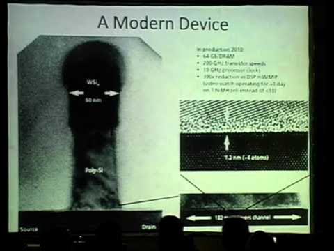
Modern computer chips are using transistors with features as small as 22nm. They are produced in factories that are 10,000 times cleaner than an operating room that can think like Skynet. Combined, the chips they produce run everything from your cell phone to the Internet itself. While outsiders might see it as the realm of multi-billion dollar corporations, in reality, it has been achieved through a hardcore application of the hacker mindset. Each new advancement involves hacking the theories of electrical engineering, hacking waves of light, and sometimes hacking physics. In this talk, we will go over how and why the design of a modern nanoscale transistor was developed. We will also talk about the processes used to build them, and the incredible equipment that makes it all possible. Plus some fun stories about what goes wrong.
[Source](https://www.youtube.com/watch?v=NGFhc8R_uO4)