Sam Zeloof Produces 1,200-Transistor Silicon Chip in Garage Fab
Sam Zeloof
A self-aligned polysilicon gate process drops threshold voltage to one volt, enabling homemade integrated circuits to run on standard digital logic rails.
AI-assisted summary of "Z2" - Upgraded Homemade Silicon Chips — original source. Check the original for full context.
Source published:
Key ideas
- Sam Zeloof introduced the Z2 integrated circuit, featuring 100 transistors per die across a 12-die array for a total of 1,200 transistors on a single homemade silicon chip. (0:00)
- A shift to a self-aligned polysilicon gate process reduced the threshold voltage to approximately 1V, enabling standard 3.3V and 5V logic compatibility without high-voltage 9V batteries. (0:00)
- Photolithography was executed using a DIY maskless stepper based on a DLP projector and a standard laptop display, eliminating expensive physical chrome reticles. (1:21)
- High-temperature drive-in diffusion at over 1000°C for 45 minutes using spin-on liquid phosphorus created the n-type source and drain wells. (3:12)
- Analytical probe station measurements confirmed textbook-grade n-channel MOSFET ID-VDS saturation and linear curves on the finished silicon. (4:40)
Detailed notes
## Background Published on YouTube by independent hardware hacker Sam Zeloof on August 13, 2021, this video showcases his upgraded homemade silicon integrated circuit fabrication process, humorously summarized as 'dipping a rock into chemicals until it becomes a computer chip.' The project log highlights his second-generation chip architecture while referencing pioneering homebrew semiconductor work by Jeri Ellsworth.
## TL;DR Sam Zeloof introduces the Z2, an upgraded homemade integrated circuit featuring a 12-die array totaling 1,200 transistors built with a self-aligned polysilicon gate process. Transitioning from high-voltage prototypes to ~1V threshold logic compatible with standard 3.3V and 5V systems, the fabrication flow relies on scribed wafer squares patterned using an innovative DIY maskless DLP projection stepper. After drive-in phosphorus diffusion in a tube furnace at over 1000°C, dielectric contact etching, and thermal evaporation of aluminum interconnects, the chip is completed and inspected under a microscope. Analytical probe testing with sub-millimeter tungsten needles verifies textbook MOSFET current-voltage curves, validating successful transistor operation from a garage cleanroom.
## Atmosphere & style The presentation is remarkably calm, methodical, and understated, presenting jaw-dropping garage engineering with the casual familiarity of a weekend workshop craft. Zeloof's soft-spoken, matter-of-fact narration demystifies advanced solid-state physics, transforming hazardous chemicals and quartz tube furnaces into approachable benchtop steps. Watching the sequence feels hypnotic and deeply satisfying, evoking quiet awe as raw silicon squares gradually reveal intricate microscopic circuitry that performs to textbook standards.
## Bulletin - [00:00](https://www.youtube.com/watch?v=IS5ycm7VfXg&t=0s) Sam Zeloof introduced the Z2 integrated circuit, featuring 100 transistors per die across a 12-die array for a total of 1,200 transistors on a single homemade silicon chip. - [00:00](https://www.youtube.com/watch?v=IS5ycm7VfXg&t=0s) A shift to a self-aligned polysilicon gate process reduced the threshold voltage to approximately 1V, enabling standard 3.3V and 5V logic compatibility without high-voltage 9V batteries. - [01:21](https://www.youtube.com/watch?v=IS5ycm7VfXg&t=81s) Photolithography was executed using a DIY maskless stepper based on a DLP projector and a standard laptop display, eliminating expensive physical chrome reticles. - [03:12](https://www.youtube.com/watch?v=IS5ycm7VfXg&t=192s) High-temperature drive-in diffusion at over 1000°C for 45 minutes using spin-on liquid phosphorus created the n-type source and drain wells. - [04:40](https://www.youtube.com/watch?v=IS5ycm7VfXg&t=280s) Analytical probe station measurements confirmed textbook-grade n-channel MOSFET ID-VDS saturation and linear curves on the finished silicon.
## Key takeaways - [00:00](https://www.youtube.com/watch?v=IS5ycm7VfXg&t=0s) The Z2 chip scales homebrew semiconductor density to 1,200 total transistors across 12 dies, approaching early commercial milestones like Intel's first processor. - [00:24](https://www.youtube.com/watch?v=IS5ycm7VfXg&t=24s) Adopting a self-aligned polysilicon gate drops threshold voltages to ~1V, allowing direct compatibility with 3.3V and 5V logic rails. - [00:47](https://www.youtube.com/watch?v=IS5ycm7VfXg&t=47s) The 4-layer mask set for the chip was designed directly in Adobe Photoshop rather than specialized EDA software. - [01:04](https://www.youtube.com/watch?v=IS5ycm7VfXg&t=64s) Production-grade 200 mm silicon wafers are cleaved into half-inch working squares using a diamond scribe to fit benchtop processing tools. - [01:21](https://www.youtube.com/watch?v=IS5ycm7VfXg&t=81s) Spin coating applies positive photoresist at 4,000 RPM for 30 seconds before a 95°C soft bake. - [01:45](https://www.youtube.com/watch?v=IS5ycm7VfXg&t=105s) A DIY maskless stepper projects blue light patterns via a DLP projector, exposing each die field in about nine seconds. - [02:08](https://www.youtube.com/watch?v=IS5ycm7VfXg&t=128s) Wafers are developed in a dilute ~2% KOH solution and can be stripped with acetone and reworked if defects appear. - [03:12](https://www.youtube.com/watch?v=IS5ycm7VfXg&t=192s) Liquid spin-on dopant containing phosphorus is diffused in a quartz tube furnace at >1000°C for 45 minutes to form n-type regions. - [03:55](https://www.youtube.com/watch?v=IS5ycm7VfXg&t=235s) Thick thermal silicon dioxide dielectric layers are etched using hydrofluoric acid or CHF3 reactive ion etching (RIE) to open contact vias. - [04:14](https://www.youtube.com/watch?v=IS5ycm7VfXg&t=254s) Approximately 1 µm of aluminum interconnect is deposited via thermal evaporation and patterned with warm phosphoric acid wet etching. - [04:40](https://www.youtube.com/watch?v=IS5ycm7VfXg&t=280s) Finished dies undergo optical inspection under a microscope to measure critical dimensions such as gate length, gate width, and film thickness. - [04:53](https://www.youtube.com/watch?v=IS5ycm7VfXg&t=293s) Micro-manipulated tungsten probe needles on an analytical station land manually on integrated pads to capture electrical characteristics. - [05:14](https://www.youtube.com/watch?v=IS5ycm7VfXg&t=314s) Automated parametric sweeps demonstrate clean ID vs. VDS curve families with distinct linear and saturation regimes matching reference textbook MOSFET behavior.
## Detailed walkthrough ### [00:00](https://www.youtube.com/watch?v=IS5ycm7VfXg&t=0s) The Z2 Chip: Architecture and Upgraded Polysilicon Process
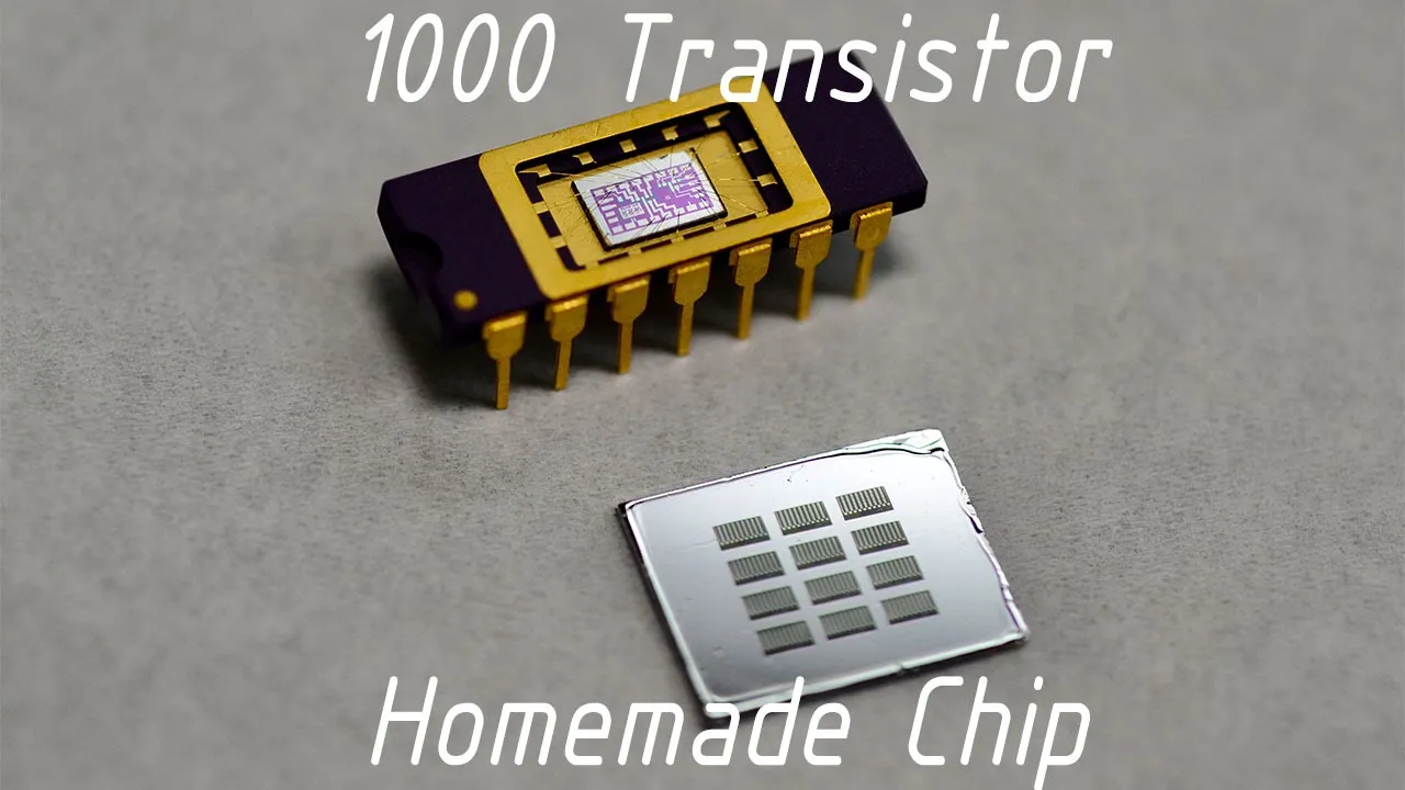
A few years after building the world's first homemade silicon chip in his garage fab, Sam Zeloof introduced the Z2, an upgraded integrated circuit featuring 100 transistors per individual die. Fabricated as an array of 12 dies across a single piece of silicon, the total transistor count reaches 1,200 devices. Reflecting on this density milestone relative to computing history, Sam Zeloof observed: “Intel's first processor had only 2,000 transistors so we're already approaching a decent level of complexity and I should be able to make some really interesting circuits out of this soon.” While earlier test projects with the first-generation chip—such as an LED flasher and a guitar distortion pedal—functioned properly, their high threshold voltages demanded one or two 9-volt batteries to operate.
The Z2 transitions to a self-aligned polysilicon gate process, fundamentally altering electrical performance. This change drops the threshold voltage down to approximately 1 volt, enabling direct compatibility with standard 3.3-volt and 5-volt logic systems, reducing total power draw, and allowing significantly tighter transistor packing inside a smaller die area. Rather than turning to heavyweight electronic design automation (EDA) software, the mask design for this four-layer process was drafted entirely in Adobe Photoshop, which proved far simpler for chips of this scale. The physical fabrication begins with 200 mm production-grade silicon wafers chosen for specific starting specifications. Because full-sized wafers are too large for the benchtop setup, they are diced with a diamond scribe into half-inch square samples, though the tooling can accommodate substrates up to two inches across.
- **Transistor count**: 100 transistors per die; 12-die array yields 1,200 transistors on a single chip. - **Operating voltage**: Drop from high-voltage 9V battery operation to ~1V threshold voltage, running on 3.3V and 5V logic rails. - **Substrate handling**: 200 mm silicon wafers cleaved down to ~0.5-inch working squares using a diamond scribe. - **Mask design**: 4 lithography layers drafted directly in Adobe Photoshop.
[01:21](https://www.youtube.com/watch?v=IS5ycm7VfXg&t=81s) Lithography and Patterning with a DIY Maskless Stepper
Patterning the first layer—the doped source and drain regions—begins on a custom-built spin coater. A tiny drop of positive photoresist, roughly 100 microliters, is dispensed onto the wafer piece and spun at 4,000 RPM for 30 seconds to produce a uniform coating. The wafer is then transferred to a hot plate for a soft bake at 95°C for one minute, driving off residual solvent carriers to leave behind an even, solid film across the silicon surface.
```mermaid flowchart TD accTitle: Z2 Photolithography Cycle accDescr: Step-by-step lithography process from resist coating through exposure, development, and etching. subgraph Coating["Resist Application"] A["Spin Coat Resist<br/>100 µL @ 4000 RPM"] --> B["Hot Plate Soft Bake<br/>95°C for 1 min"] end subgraph Exposure["Pattern Exposure"] B --> C["Maskless Stepper<br/>DLP Projection (9s)"] end subgraph Processing["Wet Processing"] C --> D["Develop in KOH<br/>~2% solution, 1 min"] D --> E["Water Rinse & Inspect<br/>Rework with acetone if needed"] E --> F["Chemical Etch<br/>Transfer pattern to film"] F --> G["Resist Strip<br/>Acetone bath"] end ```
The sensitized wafer moves to a homemade maskless photolithography stepper. Instead of expensive physical chrome-on-glass reticles, a laptop loads the mask image and feeds it to an onboard DLP projector. Projection optics reduce the image down to a miniature blue exposure field focused onto the die area. Each exposure takes about nine seconds, after which the blue light turns off and the stage steps to adjacent positions to expose the rest of the array. The exposed wafer is immersed in a dilute potassium hydroxide (KOH) developer solution (around 2%) for one minute, which washes away the exposed positive resist before being rinsed in water. Sam notes the forgiving nature of the step: if an inspection under the optical microscope reveals defects, the photoresist can simply be stripped off with acetone and recoated under adjusted exposure or development times. Once verified, the pattern is chemically etched into the underlying polysilicon layer, and the remaining resist mask is stripped away with acetone.
- **Spin coating parameters**: 100 µL positive photoresist, 4,000 RPM, 30-second cycle. - **Pre-bake**: 95°C hot plate for 60 seconds. - **Lithography system**: Maskless DLP optical reduction stepper running off a standard laptop display. - **Exposure cycle**: 9-second blue light projection per die field. - **Development**: ~2% KOH aqueous developer for ~60 seconds, followed by a DI water rinse. - **Stripping agent**: Acetone to dissolve photoresist masks after wet etching.
[03:12](https://www.youtube.com/watch?v=IS5ycm7VfXg&t=192s) High-Temperature Doping, Dielectric Etch, and Metallization
With the source and drain regions opened, the wafer is cleaned, dried, and prepared for thermal diffusion. Sam deposits a liquid spin-on dopant—phosphorus dissolved in a liquid silicon dioxide matrix—using the spin coater in the same manner as the photoresist. The wafer is loaded into a quartz diffusion tube furnace using a quartz push rod, positioning it in the hot zone at over 1000°C for approximately 45 minutes. This thermal drive-in forces phosphorus atoms deep into the exposed silicon wells, creating n-type conductive source and drain regions before the boat is pulled from the furnace tube.
```mermaid flowchart LR accTitle: Z2 High-Temperature Doping and Metallization Flow accDescr: Sequence showing dopant diffusion, gate and contact lithography, dielectric etching, and aluminum metallization. subgraph Diffusion["Doping Phase"] A["Spin-on Phosphorus"] --> B["Furnace Drive-In<br/>>1000°C, 45 min"] end subgraph GateContact["Gate & Contact Layering"] B --> C["Gate Litho & Etch<br/>Polysilicon Etchant"] C --> D["Contact Mask Litho"] D --> E["SiO2 Dielectric Etch<br/>HF or CHF3 RIE"] end subgraph Metal["Interconnect"] E --> F["Thermal Evaporation<br/>~1 µm Aluminum"] F --> G["Metal Lithography"] G --> H["Phosphoric Acid Etch<br/>Warm bath"] end ```
The complete photolithographic sequence—spin coating, soft baking, stepper exposure, and development—is repeated twice more to form the gate and contact levels. The gate layer is etched using polysilicon wet etchant. Because the 1000°C diffusion stage leaves a thick, insulating layer of silicon dioxide across the entire surface, the contact vias require an aggressive dielectric removal process using either hydrofluoric acid (HF) wet etching or carbon trifluoride (CHF3) reactive ion etching (RIE) to uncover bare silicon for low-resistance connections. The wafer is then placed inside a high-vacuum chamber where a thick layer of aluminum (approximately one micron) is deposited, primarily via thermal evaporation. A final round of photolithography patterns the metal interconnect traces, followed by immersion in a warm phosphoric acid bath to strip residual aluminum and isolate the circuits.
- **Dopant chemistry**: Phosphorus suspended in liquid silicon dioxide (spin-on dopant). - **Drive-in diffusion**: >1000°C tube furnace for 45 minutes using quartz tooling. - **Dielectric oxide stripping**: Hydrofluoric acid (HF) dip or CHF3 reactive ion etching (RIE). - **Metallization thickness**: ~1 µm thermally evaporated aluminum layer. - **Metal etching**: Warm phosphoric acid bath.
[04:40](https://www.youtube.com/watch?v=IS5ycm7VfXg&t=280s) Wafer Inspection, Probe Testing, and Transistor Characterization
Once metal etching is complete, the finished wafer undergoes detailed optical inspection under a microscope. Sam captures high-magnification photomicrographs to verify alignment and measure critical dimensions, including gate length, gate width, and film thicknesses, occasionally checking cross-sections. Electrical testing takes place on an analytical probe station equipped with micro-positioners holding extremely fine tungsten needles, which must be manually landed on tiny contact pads. Highlighting the physical difficulty of this stage, Sam remarks: “It's very finicky and these transistors are so small that it's not actually that trivial to make contact to them but anyway I boot up all this test equipment that allows me to characterize them.”
Automated parametric test instruments, controlled via custom test software, sweep voltages across the terminal pins to evaluate device physics. The key readout is the drain current versus drain-to-source voltage ($I_D$ vs. $V_{DS}$) curve family across varying gate biases for the homemade n-channel MOSFETs. When plotted, the output curves display clean saturation plateaus and sharp linear regimes that closely match ideal textbook curves sourced from reference literature. Satisfied with the yield and gate control of the Z2 architecture, Sam concludes by addressing viewer interest in funding garage fabrication hardware, noting that a Patreon link has been established to support future homebrew semiconductor experiments.
- **Inspection targets**: Gate width, gate length, layer alignment, cross-sectional thickness. - **Probe setup**: Micro-manipulated tungsten needles contacting miniature integrated pads. - **Electrical validation**: $I_D$ versus $V_{DS}$ curve family confirms proper n-channel MOSFET operation and active pinch-off/saturation behavior.
## Notable quotes > [00:00](https://www.youtube.com/watch?v=IS5ycm7VfXg&t=0s) Intel's first processor had only 2,000 transistors so we're already approaching a decent level of complexity and I should be able to make some really interesting circuits out of this soon. — Sam Zeloof
## Mentioned Sam Zeloof, Z2, Intel, Adobe Photoshop, Jeri Ellsworth, Patreon, YouTube
## Video description https://www.patreon.com/szeloof
http://sam.zeloof.xyz/second-ic/
Check our Jeri Ellsworth's amazing work making the first transistors and logic gates at home https://www.youtube.com/watch?v=PdcKwOo7dmM&t=1s
Dipping a rock into chemicals until it becomes a computer chip Upgraded Homemade Silicon IC Fab Process
[Source](https://www.youtube.com/watch?v=IS5ycm7VfXg)