ASML masters EUV plasma physics to extend Moore's Law chip shrink
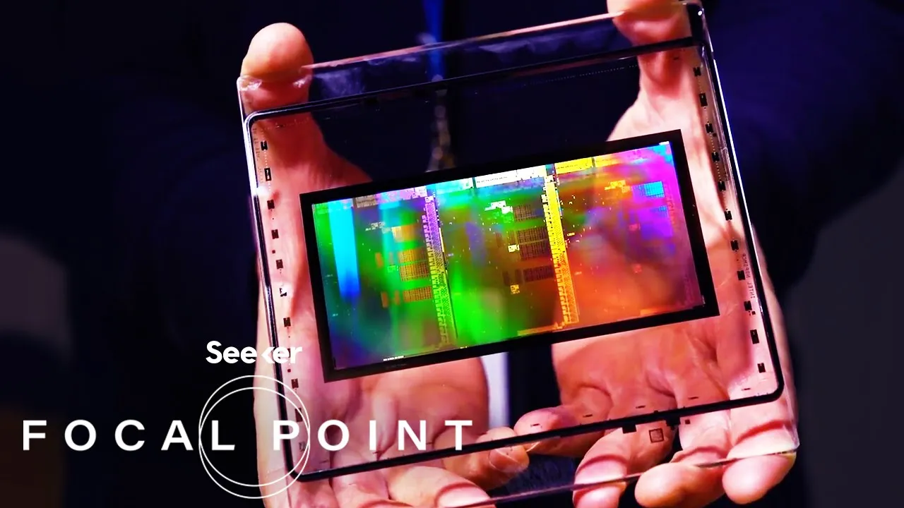
The Extreme Physics Pushing Moore’s Law to the Next Level — Seeker

Seeker

ASML overcame decades of industry skepticism by deploying a synchronized dual-pulse laser to vaporize molten tin into extreme ultraviolet plasma, unlocking the optical power needed to manufacture sub-10nm chips.

AI-assisted summary of The Extreme Physics Pushing Moore’s Law to the Next Level — original source. Check the original for full context.

Source published:

Key ideas

  • Extreme Ultraviolet (EUV) lithography shifts the semiconductor exposure wavelength from 193 nm down to 13.5 nm, enabling chipmakers to print sub-10nm nanoscale features onto silicon wafers. (5:03)
  • ASML overcame years of power conversion bottlenecks around 2015 by introducing a dual-pulse laser system that shapes molten tin droplets before vaporizing them into 13.5 nm plasma. (7:46)
  • An EUV scanner weighs over 180,000 kilograms across 100,000 components, requiring 40 freight containers, 20 cargo trucks, and 3 Boeing cargo aircraft to transport. (8:55)
  • Because 13.5 nm light is absorbed by air and glass, the entire optical path must operate within an absolute vacuum using reflective multilayer mirrors rather than transmissive lenses. (5:39)

Detailed notes

## Background This video was published on October 27, 2019, by the science channel Seeker on YouTube as an episode of their series *Focal Point*. According to the description, it explores the cutting-edge, precision EUV lithography machines that are reinventing the chip-making industry and driving Moore's Law forward into sub-nanometer territory.

## TL;DR The episode examines the technological evolution of semiconductor manufacturing, tracing how photolithography pushed through physical barriers from optical wavelengths to deep ultraviolet immersion. Facing the limits of light refraction, Netherlands-based ASML pioneered Extreme Ultraviolet (EUV) lithography, utilizing a 13.5-nanometer wavelength generated by vaporizing microscopic molten tin droplets with dual-pulsed lasers inside a vacuum. Despite widespread industry skepticism and decades of engineering dead ends, EUV transitioned into high-volume manufacturing, keeping Moore's Law alive to power the next generation of mobile computing and scientific data analysis.

## Atmosphere & style The presentation carries an awe-inspiring, reverent tone that balances industrial spectacle with deeply intricate physics. Viewers are guided through quiet, sterile cleanrooms where engineers speak with palpable humility and nervous respect regarding machines so complex they cause lost sleep. The narrative arc builds from decades of skepticism and near-failures into a triumphant technological vindication, evoking wonder at human persistence and atomic-level precision.

## Bulletin - [05:03](https://www.youtube.com/watch?v=f0gMdGrVteI&t=303s) Extreme Ultraviolet (EUV) lithography shifts the semiconductor exposure wavelength from 193 nm down to 13.5 nm, enabling chipmakers to print sub-10nm nanoscale features onto silicon wafers. - [07:46](https://www.youtube.com/watch?v=f0gMdGrVteI&t=466s) ASML overcame years of power conversion bottlenecks around 2015 by introducing a dual-pulse laser system that shapes molten tin droplets before vaporizing them into 13.5 nm plasma. - [08:55](https://www.youtube.com/watch?v=f0gMdGrVteI&t=535s) An EUV scanner weighs over 180,000 kilograms across 100,000 components, requiring 40 freight containers, 20 cargo trucks, and 3 Boeing cargo aircraft to transport. - [05:39](https://www.youtube.com/watch?v=f0gMdGrVteI&t=339s) Because 13.5 nm light is absorbed by air and glass, the entire optical path must operate within an absolute vacuum using reflective multilayer mirrors rather than transmissive lenses.

## Key takeaways - [00:02](https://www.youtube.com/watch?v=f0gMdGrVteI&t=2s) The EUV lithography tool is an engineering marvel the size of a school bus, containing over 100,000 components, 3,000 interconnect cables, and weighing over 180,000 kilograms. - [00:54](https://www.youtube.com/watch?v=f0gMdGrVteI&t=54s) Moore's Law functions as an industry expectation and pace of innovation—doubling transistor density roughly every two years—rather than a strict physical law. - [02:08](https://www.youtube.com/watch?v=f0gMdGrVteI&t=128s) Photolithography evolved across shrinking light wavelengths, progressing from 365 nm down through 248 nm and 193 nm before hitting physical barriers. - [02:40](https://www.youtube.com/watch?v=f0gMdGrVteI&t=160s) The semiconductor industry spent hundreds of millions of dollars attempting to deploy 157 nm lithography before the approach ultimately failed. - [02:58](https://www.youtube.com/watch?v=f0gMdGrVteI&t=178s) Immersion lithography extended 193 nm tools by placing a water puddle between the final lens and wafer, compressing the light while moving stages at 700 mm per second. - [05:03](https://www.youtube.com/watch?v=f0gMdGrVteI&t=303s) Transitioning to EUV represents a disruptive jump into soft X-ray physics at 13.5 nm, which was required because immersion reached its physical scaling limits. - [05:39](https://www.youtube.com/watch?v=f0gMdGrVteI&t=339s) Because matter and air absorb 13.5 nm light, EUV scanners must operate in an ultra-high vacuum environment utilizing exclusively reflective mirrors instead of refractive lenses. - [06:16](https://www.youtube.com/watch?v=f0gMdGrVteI&t=376s) The EUV light source fires high-speed molten tin droplets narrower than a human hair into a vacuum, striking them with pulsed lasers with sub-micron precision. - [07:24](https://www.youtube.com/watch?v=f0gMdGrVteI&t=444s) The synchronized 200-kilogram wafer stage accelerates faster than a modern fighter jet during the step-and-scan lithography process. - [07:46](https://www.youtube.com/watch?v=f0gMdGrVteI&t=466s) Source power efficiency stalled EUV progress until ASML implemented a dual-pulse laser technique in 2015, using a pre-pulse to flatten the droplet before vaporization. - [08:35](https://www.youtube.com/watch?v=f0gMdGrVteI&t=515s) Cleanroom technicians wear bunny suits primarily to protect the silicon wafers and optics from shedding human skin cells and fibers, not to protect the humans. - [08:55](https://www.youtube.com/watch?v=f0gMdGrVteI&t=535s) Logistical deployment of a single EUV scanner requires 40 freight containers, 20 trucks, and 3 Boeing cargo planes. - [11:06](https://www.youtube.com/watch?v=f0gMdGrVteI&t=666s) Exponential growth in data from modern scientific experiments requires continued semiconductor scaling to build computers capable of processing the results.

## Detailed walkthrough ### [00:02](https://www.youtube.com/watch?v=f0gMdGrVteI&t=2s) An Engineering Marvel the Size of a School Bus

Entering the specialized clean rooms where the future of computing is built reveals a machine of intimidating scale and complexity. Engineers view these systems with equal parts awe and anxiety, as one insider explains: “They're both amazing machines and scary machines. There's an enormous amount of complexity with them. There's an enormous number of things that can potentially go wrong. It's something that you don't necessarily sleep well at night, just having the machine on your floor.”

The machine is roughly the size of a standard school bus and represents an extraordinary feat of physical assembly. Under the hood, ultra-precise lasers target microscopic droplets of molten tin, vaporizing them into high-energy plasma. This plasma emits extreme ultraviolet radiation that is collected and directed by a specialized series of mirrors to imprint nanoscale circuit patterns onto silicon wafers—patterns destined for the next generation of mobile devices and consumer hardware. Debuting after three decades of relentless breakthroughs across physics, chemistry, and materials science, the tool stands at the absolute vanguard of semiconductor manufacturing.

- **Weight:** Over 180,000 kilograms - **Components:** More than 100,000 individual parts - **Cabling:** 3,000 interlocking interconnect cables - **Core Mechanism:** Laser-induced tin plasma generating light collected by precision optics to etch nanoscale features

---

[00:54](https://www.youtube.com/watch?v=f0gMdGrVteI&t=54s) Turning Sand into Gold: Moore's Law and Scaling Limits

The integrated circuit transformed global society throughout the 20th century, sparking the modern computing revolution, establishing Silicon Valley, and putting miniature supercomputers into billions of pockets. When examined at extreme magnification, a microchip resembles an exquisitely arranged, nanoscale metropolis engineered to route electronic information. Semiconductor lithography acts as modern alchemy, converting humble silicon into devices of immense economic and technological value. Transistors serve as the foundational switches, turning electron flows on and off to execute the binary code (zeros and ones) of computation. By stacking complex layers of wiring, gates, and insulators, engineers turn raw silicon into dense functional networks.

At tech showcases, chipmakers frequently celebrate shrinking process nodes from 22 nanometers down to 14nm and 10nm. These generational reductions allow more transistors to occupy the same footprint, driving overall processing power upward under the industry's defining cadence: Moore's Law. As one engineer observes: “Moore's Law is an expectation. It's not a natural law. It's an expectation that we innovate at a pace of roughly doubling the density every two years.” Despite decades of doomsday forecasts, the rule has endured: “Moore's Law has been predicted to be dying for a long time and yet it never is. Because each generation of engineers knows it's their expectation to keep working on it, to keep going at a certain pace.”

```mermaid flowchart LR accTitle: The Semiconductor Photolithography Flow accDescr: Light travels from a laser source through a reticle blueprint and optics to pattern a silicon wafer. subgraph Illumination["Light Generation"] A["Laser Source<br/>(Excited Gas Mixture)"] --> B["Specific Wavelength Beam"] end subgraph Masking["Pattern Masking"] B --> C["Mask / Reticle<br/>(Circuit Blueprint)"] end subgraph Projection["Wafer Exposure"] C --> D["Projection Optics / Water Gap"] D --> E["Silicon Wafer Stage<br/>(Billion-Transistor Print)"] end ```

- **Photolithography Analogy:** Functions like darkroom photography, substituting photographic film negatives with a circuit blueprint known as a mask or reticle. - **Laser Gas Mixtures:** Conventional systems utilize excited gases such as carbon dioxide or argon fluoride (ArF) energized by electric currents. - **Wavelength Evolution:** Lithography light progressed from 365 nm (mercury i-line) down to 248 nm (krypton fluoride laser) and 193 nm (argon fluoride laser). Visible light spans roughly 400 to 650 nm. - **The 157 nm Failure:** The industry spent hundreds of millions of dollars attempting to develop a 157 nm light source, but the effort failed, forcing engineers to find clever optical workarounds. - **Immersion Lithography:** Engineers bypassed wavelength limits by injecting a thin puddle of water between the final lens element and the wafer. Because light compresses inside water, the effective resolution improved, despite initial industry doubts: “When I first heard about it, I thought it was just crazy. You're going to get water all over the stages, and the electronics inside the tool.” - **Wafer Velocity:** Immersion stages manage to retain the liquid barrier while moving the wafer back and forth at roughly 700 millimeters per second.

---

[05:03](https://www.youtube.com/watch?v=f0gMdGrVteI&t=303s) The Leap to EUV and ASML’s Radical Architecture

Immersion lithography eventually hit a physical barrier where it could no longer resolve finer features without introducing severe manufacturing defects. To sustain Moore's Law without violating physical laws, the industry pivoted toward Extreme Ultraviolet (EUV) lithography. EUV slashes the exposure wavelength from 193 nanometers all the way down to 13.5 nanometers. This was not an incremental step; it represented a massive, disruptive technological leap into soft X-ray territory.

Although initial academic inquiries into EUV began as early as 1986, turning theoretical physics into an industrial production tool took decades of development. At sub-10nm scales, manufacturing margins are so narrow that feature variation is quantified at the atomic level. Netherlands-based ASML led this effort, designing an entirely new architecture from the ground up: “ASML is the most important tech company you've never heard of. We build the big machines that make small chips. EUV was a massive step for us to undertake.” Because 13.5 nm light is absorbed by almost all matter—including air and traditional glass transmission lenses—the scanner must operate inside an absolute vacuum using exclusively reflective multilayer mirrors.

| Parameter | Deep Ultraviolet (DUV) Immersion | Extreme Ultraviolet (EUV) | |:--- |:--- |:--- | | **Exposure Wavelength** | 193 nanometers | 13.5 nanometers | | **Optical Medium** | High-purity water puddle & refractive glass lenses | High-vacuum chamber & reflective multilayer mirrors | | **Light Source** | Argon fluoride (ArF) excimer laser | High-power pulsed laser firing on molten tin droplets | | **Optical Configuration** | Transmissive optics | Multi-mirror reflective collector, shaping slits, & reticle |

- **Design Challenge:** Marked the first time lithography engineers had to overhaul the scanner's internal optics and construct a completely novel light source simultaneously. - **Source Mechanics:** Microscopic molten tin droplets, significantly narrower than a human hair, are injected into a vacuum chamber at highway speeds. - **Targeting Precision:** The pulsed laser beam must strike these high-speed tin droplets with sub-micron spatial accuracy. - **Optics Layout:** A collector mirror captures the emitted 13.5 nm plasma radiation, routing it through four shaping mirrors that focus the light into an exposure slit across the reflective reticle. - **Wafer Stage Dynamics:** In a coordinated "step and scan" motion, the reticle stage and wafer stage move in absolute synchronization; despite weighing approximately 200 kilograms, the wafer stage accelerates faster than a modern fighter jet.

---

[07:46](https://www.youtube.com/watch?v=f0gMdGrVteI&t=466s) Cracking the Dual-Pulse Physics and High-Volume Manufacturing

The most daunting obstacle that fueled industry skepticism was generating sufficient optical source power for commercial manufacturing. For years, low EUV source power stalled system throughput at commercially non-viable levels, with rollout schedules slipping year after year. Engineers were forced to return to primary plasma physics to diagnose why conversion efficiency remained capped.

Around 2015, ASML cracked the fundamental problem by moving from a single laser blast to a synchronized double-pulse strategy. The first "pre-pulse" laser hits the spherical tin droplet, flattening and shaping it into an optimal geometric target. Microseconds later, the main high-power laser pulse vaporizes the expanded target into an ultra-hot plasma cloud, drastically raising the power conversion efficiency at 13.5 nm.

```mermaid flowchart TD accTitle: Dual-Pulse Laser-Produced Plasma Process accDescr: The two-stage laser firing sequence that turns a molten tin droplet into 13.5 nm EUV plasma. A["Droplet Generator fires microscopic tin droplet into vacuum"] --> B["Pre-Pulse Laser strikes tin droplet"] B --> C["Droplet flattens and shapes into optimal target disc"] C --> D["High-Power Main Laser Pulse strikes shaped tin"] D --> E["Ultra-Hot Plasma generates 13.5 nm EUV light"] E --> F["Collector Mirror captures EUV light into scanner optics"] ```

To protect these sensitive optical systems from stray debris, spotless cleanroom discipline is mandatory. Humans are the primary vector for particulate contamination; unless an internal mechanical stage scrapes or malfunctions, cleanroom machinery emits virtually zero dust. Technicians must wear protective cleanroom bunny suits entirely to shield the equipment and wafers from human-shed skin cells and fibers, rather than to protect the technicians themselves.

Shipping an EUV machine from ASML's manufacturing centers requires a vast logistical operation involving 40 freight containers, 20 cargo trucks, and 3 Boeing cargo transport planes. Despite years of skepticism from leading physicists who argued a practical EUV tool was commercially impossible, the technology has transitioned into high-volume semiconductor manufacturing. EUV-patterned microchips are now driving modern cloud servers, smartphones, and cutting-edge research facilities—including next-generation particle accelerators designed to log trillions of subatomic collision events. As an engineer reflects on the monumental journey: “The EUV scanner is the most technically advanced tool of any kind, that's every been made. It's so far from normal human experience. I can't think of anything that has pushed the envelope in so many areas. There were many knowledgeable people in the field who just said, 'You can never make a practical tool this way.'”

[11:06](https://www.youtube.com/watch?v=f0gMdGrVteI&t=666s) Computing the Future One Step at a Time

The sheer volume of information being generated across the scientific landscape has outpaced what current hardware can process. Even the latest generation of computer systems cannot fully digest and interpret the torrent of data flooding in each second, creating an urgent demand for hardware acceleration. As the speaker explains, “So you've got to go build ever faster computers, larger data storage, just to make sense of the science that's going on.” Advancing semiconductor technology is not merely an engineering benchmark; it is the prerequisite for unlocking discoveries hidden inside modern scientific experiments.

Looking ahead, diagnosing technological trends is central to forecasting where computing is headed. While stepping into the unknown can be daunting, the speaker views the uncertainty of the future not with apprehension, but as an opportunity for innovation: “If you don't know what the future holds, are you afraid of that or are you encouraged by it? And I'm in the category of being encouraged by it because there's things to do that you haven't done before, things to create that you haven't created before.” Progress does not require an all-at-once revolution; rather, technological frontiers expand through continuous, methodical engineering breakthroughs that reshape civilization incrementally: “And then you may not set out to change the world, but we changed the world one step at a time.”

## Notable quotes > [00:54](https://www.youtube.com/watch?v=f0gMdGrVteI&t=54s) Moore's Law is an expectation. It's not a natural law. It's an expectation that we innovate at a pace of roughly doubling the density every two years.

## Mentioned ASML, Intel, Samsung, TSMC, Gordon Moore, Robert Noyce, Moore's Law, EUV lithography, Silicon Valley, Boeing

## Video description A look inside a new precision machine that wants to reinvent the chip making industry. »Subscribe to Seeker! http://bit.ly/subscribeseeker »Watch more Focal Point |https://bit.ly/31Ms6mj

An integrated circuit, or chip, is one of the biggest innovations of the 20th century. The microchip launched a technological revolution, created Silicon Valley, and everyone’s got one in their pocket (read: smartphones).

When you zoom in on one of these chips, you find a highly complex, nanoscale-sized city that’s expertly designed to send information back and forth.

And chip manufacturers continue to shrink the size of microchips, hitting smaller and smaller milestones while also increasing the number of features a chip has. The result is an improved overall processing power.

This is what’s been driving the semiconductor industry—a drumbeat called Moore’s Law.

Moore's Law is the golden rule in computing: The number of transistors on a microchip can be expected to double every two years, while the cost of computers is cut in half. This basically means we'll have more speed, at less cost, over time. And so, we've been shrinking transistors (the tiny electric switches that process data for everything from clocks to AI algorithms) down to really, really tiny nanoscales.

And though we've hit a physical limit on how small these transistors can get, Intel (and a couple other competitors, like Samsung and TSMC) are betting big on something new: EUV Lithography.

Find out more about this next generation of chip technology that is taking Moore’s Law to a new level on this episode of Focal Point.

#MooresLaw #MicroChip #SiliconValley #Computing #EUVLithography #Seeker #FocalPoint #Science ____________________

Read More:

EUV Lithography Finally Ready for Chip Manufacturing https://spectrum.ieee.org/semiconductors/nanotechnology/euv-lithography-finally-ready-for-chip-manufacturing “The giant machine garnering all this attention is an extreme ultraviolet lithography tool. For more than a decade, the semiconductor-manufacturing industry has been alternately hoping EUV can save Moore’s Law and despairing that the technology will never arrive. But it’s finally here, and none too soon.”

Moore's Law Keeps Going, Defying Expectations https://www.scientificamerican.com/article/moore-s-law-keeps-going-defying-expectations/ “It’s a mystery why Gordon Moore’s “law,” which forecasts processor power will double every two years, still holds true a half century later”

Silicon Valley Owes Its Success To This Tech Genius You’ve Never Heard Of https://www.smithsonianmag.com/smart-news/silicon-valley-owes-its-success-tech-genius-youve-never-heard-180961395/ “They called Robert Noyce the Mayor of Silicon Valley, but like many in public office, his work wasn’t well known.” ____________________

Our scientific understanding of the universe is advancing at an unprecedented rate. Join Focal Point as we meet the people building tomorrow’s world. Witness the astonishing discoveries that will propel humanity forward and zero-in on the places where science-fiction becomes science-reality.

Seeker empowers the curious to understand the science shaping our world. We tell award-winning stories about the natural forces and groundbreaking innovations that impact our lives, our planet, and our universe.

Visit the Seeker website https://www.seeker.com

Seeker on Facebook https://www.facebook.com/SeekerMedia/

Focal Point on Facebook https://www.facebook.com/FocalPointShow/

Seeker on Twitter http://twitter.com/seeker

[Source](https://www.youtube.com/watch?v=f0gMdGrVteI)

中文简报

ASML攻克EUV等离子体物理难题,延续摩尔定律芯片微缩 ASML通过应用同步双脉冲激光将熔融锡气化为极紫外等离子体,克服了业内数十年的质疑,释放出制造10纳米以下芯片所需的光功率。 本期内容探讨了半导体制造的技术演进,追溯了光刻技术如何突破物理障碍,从光学波长迈向深紫外浸润式技术。面对光折射的物理极限,总部位于荷兰的ASML率先开创了极紫外(EUV)光刻技术,该技术利用在真空中通过双脉冲激光气化微观熔融锡滴所产生的13.5纳米波长。尽管面临业界的广泛怀疑以及数十年的工程死胡同,EUV仍成功迈入大规模量产阶段,延续了摩尔定律,为下一代移动计算和科学数据分析提供动力。 极紫外(EUV)光刻将半导体曝光波长从193纳米缩短至13.5纳米,使芯片制造商能够在硅晶圆上印制10纳米以下的纳米级特征。 (5:03) ASML在2015年左右通过引入双脉冲激光系统克服了多年的功率转换瓶颈,该系统在将熔融锡滴气化为13.5纳米等离子体之前先对其进行塑形。 (7:46) 一台EUV光刻机包含10万个零部件,重量超过18万公斤,运输需要40个货运集装箱、20辆货车和3架波音货机。 (8:55) 由于13.5纳米的光会被空气和玻璃吸收,整个光路必须在完全真空的环境下运行,并使用反射式多层膜反射镜而非透射式透镜。 (5:39)

Reading summary

To sustain Moore's Law beyond the physical limits of conventional optical lithography, semiconductor manufacturing shifted to extreme ultraviolet (EUV) systems that utilize soft X-ray wavelengths, vacuum optics, and laser-produced plasma. According to industry engineers, converting these complex physics into high-volume tools was deemed nearly impossible by critics, but it has become essential for processing modern scientific and commercial data. Evolutionary Limits of Optical Lithography (0:54) Moore's Law functions not as a law of nature, but as an industry expectation to roughly double transistor density every two years. To maintain this cadence, photolithography systems initially progressed down the electromagnetic spectrum from 365-nanometer mercury i-line light to 248-nanometer krypton fluoride and 193-nanometer argon fluoride excimer lasers. However, direct wavelength scaling stalled when a multi-million-dollar industry initiative to develop a 157-nanometer light source failed entirely. To postpone physical limits without altering the light source, engineers developed immersion lithography, inserting a puddle of high-purity water between the final lens element and the wafer. Because light compresses in water, this technique significantly improved optical resolution while retaining liquid stability on stages moving at roughly 700 millimeters per second. Despite these workarounds, immersion lithography eventually reached an insurmountable physical barrier where further miniaturization caused severe manufacturing defects. Radical Vacuum Architecture for Extreme Ultraviolet (5:03) Overcoming the scaling barrier required a direct transition to Extreme Ultraviolet (EUV) lithography at a 13.5-nanometer wavelength—a disruptive leap into soft X-ray physics led by Netherlands-based ASML. Because 13.5-nanometer radiation is absorbed by virtually all matter, including ambient air and traditional transmissive glass lenses, the entire optical track must operate inside a high-vacuum chamber using specialized reflective multilayer mirrors. The resulting production tool weighs over 180,000 kilograms and integrates more than 100,000 components and 3,000 interconnect cables. In coordinated step-and-scan operations, precision collector and shaping mirrors focus EUV light onto a reflective reticle. Synchronized beneath the optics, the system's 200-kilogram wafer stage accelerates faster than a modern fighter jet to pattern silicon at atomic tolerances. Overcoming Power Limits with Dual-Pulse Lasers (7:46) Commercial viability was long delayed by insufficient optical source power, which suppressed wafer throughput and prompted skepticism from physicists who doubted a practical EUV scanner could ever operate in high-volume manufacturing. ASML resolved this limitation around 2015 by abandoning single laser pulses in favor of a synchronized dual-pulse firing sequence targeting microscopic droplets of molten tin. In this architecture, tin droplets narrower than a human hair are shot into the vacuum chamber at highway speeds. A low-energy pre-pulse laser strikes each droplet first, flattening it into a wider target disc. Microseconds later, a high-power main laser pulse vaporizes the shaped droplet into an ultra-hot plasma cloud that emits 13.5-nanometer radiation with high power conversion efficiency. Strict cleanroom protocols, including technician bunny suits designed to contain human-shed skin and fibers, prevent particulate contamination from damaging the optical collector and reflective surfaces. Scientific Data Pressures and Incremental Frontiers (11:06) High-volume EUV manufacturing now patterns chips powering commercial cloud infrastructure, consumer hardware, and large-scale experimental facilities, such as particle accelerators logging trillions of subatomic collisions. System engineers emphasize that the exponential accumulation of scientific data has outpaced current computational capabilities, making advanced semiconductor scaling an operational necessity to analyze experimental findings. Industry insiders argue that technological progress in computing does not depend on immediate revolutions, but on continuous, methodical engineering breakthroughs. Despite historical doomsday predictions regarding the demise of Moore's Law, engineers view unresolved physical challenges as an incentive for ongoing innovation, sustaining computing growth one deliberate step at a time. While the commercial realization of EUV lithography resolved decades of industry skepticism, sustained scaling remains constrained by the rising computational demands of modern experimental science. Future progress relies on continued, incremental engineering across materials science, mechanics, and plasma physics to prevent data generation from permanently outpacing processing capacity.

精炼阅读摘要

节目指出,摩尔定律并非物理法则,而是一种驱动半导体行业每两年将芯片密度翻倍的行业预期;为了突破传统光学光刻的物理瓶颈,ASML等企业历经数十年研发,成功将极紫外光刻(EUV)推向商业量产。 从浸没式光刻到波长物理极限 (0:54) 半导体光刻技术通过将电路蓝图投影到硅片上制造晶体管。在演进过程中,光源波长从365纳米逐步缩短至248纳米与193纳米(氟化氩激光)。然而,行业耗资数亿美元研发157纳米光源的尝试最终宣告失败,促使工程师转向光学替代方案。随后出现的浸没式光刻技术在最终透镜与晶圆之间注入高纯度水薄层,利用光在水中的压缩特性提升有效分辨率,同时晶圆台在保持水液边界的状态下以约每秒700毫米的速度往返移动。尽管浸没式光刻延缓了危机,但随着晶体管特征尺寸向10纳米以下微缩,该技术最终遭遇了无法避免严重制造缺陷的物理极限。 极紫外光刻的真空与反射式架构 (5:03) 为延续芯片微缩,半导体产业转向极紫外(EUV)光刻,将曝光波长从193纳米直接骤降至13.5纳米的软X射线波段。荷兰ASML主导了这一全新系统架构的开发。由于几乎所有物质(包括空气与传统透光玻璃透镜)都会吸收13.5纳米光线,光刻机必须在高度真空的腔体内运行,且全部采用特制的多层反射镜。整机系统重达180多吨,包含超过10万个零部件与3000根互连电缆,尺寸堪比一辆标准校车。在精密步进扫描运动中,重约200公斤的晶圆台以超越现代喷气式战斗机的加速度移动,且必须与掩模台保持绝对同步。 双脉冲激光等离子体突破量产瓶颈 (7:46) 长期制约EUV商业化落地的核心难题在于光源功率不足,导致生产吞吐量多年达不到商业化可行标准。2015年前后,ASML通过重构等离子体物理机制打破了这一瓶颈,由单脉冲轰击改为双脉冲激光策略:第一道预脉冲激光击中以极高速射入真空腔的微米级熔融锡滴,将其压平并塑形为理想靶盘;微秒之后,高功率主脉冲激光轰击已形变的锡靶,将其彻底汽化为极高温等离子体云,从而大幅提升13.5纳米极紫外光的能量转换效率。反射收集镜随后捕获该辐射光,通过整形反射镜投射到反射式光掩模上。 超净环境管控与极限制程物流落地 (7:46) 由于亚10纳米制程对原子级别的缺陷极其敏感,保护昂贵的光学元件免受微粒污染至关重要。洁净室内的机械系统除刮擦或故障外几乎不排放粉尘,人类自身则是微粒污染的主要来源;因此技术人员穿戴全封闭防尘服,实质是为了阻隔人体脱落的皮屑与纤维污染设备和晶圆。完成制造的EUV光刻机在运输上面临极限后勤挑战,单台设备出厂需要动用40个货运集装箱、20辆货车以及3架波音货机联合转运。曾经被部分物理学家判定为无法实用的工具,现已正式进入大规模量产,应用于先进制程芯片制造。 现代科学实验与计算所产生的数据洪流已经超出当前硬件的处理能力,持续推进半导体制造是支撑未来科学发现的必要基础;受访工程师认为,未来的技术边界将通过持续、渐进的工程突破来逐步拓展。

Detailed notes — zh

## Background 本内容由科普频道 Seeker 于 2019 年 10 月 27 日发布在 YouTube 平台上的《Focal Point》专栏节目中。视频简介指出,节目将带领观众走进一台试图重塑芯片制造产业的超精密机器,深入探究将摩尔定律推向全新极限的下一代芯片技术——极紫外光刻(EUV Lithography)。 ## TL;DR 微芯片作为现代计算与硅谷的核心引擎,长期依赖摩尔定律所驱动的晶体管微缩与性能倍增,然而传统光刻技术在缩短波长至深紫外浸润式(193 纳米)后已逼近物理极限。为了继续推进工艺节点,荷兰光刻设备巨头 ASML 历经三十年研发攻关,研发出采用 13.5 纳米软 X 射线的极紫外光刻机,并在真空腔体内通过两发激光脉冲高速精准轰击液态锡滴,成功解决了极端光源转换效率的死穴。如今,这台重达 180 吨、需要出动多架运输机运送的精密工业奇迹已迈入规模化商业量产,为云计算与尖端科学研究中的海量数据处理提供强大的算力支撑。 ## Atmosphere & style 全片洋溢着宏大震撼的硬核工业史诗感与严谨求实的科学探索氛围。通过带领观众穿戴防尘服步入神秘的半导体无尘室,镜头语言巧妙结合了庞大复杂的机械骨架与微观尺度的等离子体爆发,形成强烈的视听张力。专家受访时在沉稳理性的技术拆解中流露出攻克三十年物理死穴后的自豪与敬畏,情绪从面对未知物理极限的严峻挑战,逐步走向跨学科协同破局的昂扬振奋,给观众带来一种亲眼见证现代工业文明最巅峰奇迹的真实战栗感。 ## Bulletin - [05:12](https://www.youtube.com/watch?v=f0gMdGrVteI&t=312s) ASML 成功商用 EUV 极紫外光刻机,将半导体曝光波长从深紫外的 193 纳米断崖式缩短至 13.5 纳米软 X 射线波段,打破摩尔定律面临的物理极限。 - [07:46](https://www.youtube.com/watch?v=f0gMdGrVteI&t=466s) EUV 光源通过双脉冲激光方案突破功率瓶颈:第一发预脉冲将微米级液态锡滴压扁成饼状,第二发高能主脉冲将其完全电离为高温等离子体,大幅提升能量转换效率。 - [09:03](https://www.youtube.com/watch?v=f0gMdGrVteI&t=543s) EUV 设备整机重量超 180 吨并包含超 10 万个精密零部件,单台交付需要动用 40 个大型集装箱、20 辆重型卡车以及 3 架货运飞机协同运输。 - [03:00](https://www.youtube.com/watch?v=f0gMdGrVteI&t=180s) 在进入 EUV 时代前,半导体行业在 157 纳米干式光刻沉没数亿美元后转向浸润式技术,利用水介质将 193 纳米激光等效缩减至 134 纳米并支撑了工件台每秒 700 毫米的高速扫描。 ## Key takeaways - [00:02](https://www.youtube.com/watch?v=f0gMdGrVteI&t=2s) 摩尔定律本质上并非不可违背的自然物理法则,而是半导体行业约每两年将芯片晶体管密度翻倍的共同预期与经济驱动力。 - [03:00](https://www.youtube.com/watch?v=f0gMdGrVteI&t=180s) 光刻工艺的物理分辨率取决于光波波长,波长越短衍射极限越小,芯片表面可刻蚀的电路密度和晶体管数量就越高。 - [03:00](https://www.youtube.com/watch?v=f0gMdGrVteI&t=180s) 在 157 纳米光刻路线因材料吸收率过高而失败后,业界通过在物镜与晶圆间注入纯净水的浸润式光刻,将 193 纳米激光等效缩短至约 134 纳米延续制程。 - [05:12](https://www.youtube.com/watch?v=f0gMdGrVteI&t=312s) 13.5 纳米的 EUV 极紫外光会被空气及普通光学玻璃强烈吸收,因此整台机器必须运行在超高真空环境中,并完全采用全反射多层膜光学系统代替传统透镜折射。 - [05:12](https://www.youtube.com/watch?v=f0gMdGrVteI&t=312s) EUV 光刻机的研发是半导体工业史上首次在彻底重构扫描机机械与真空架构的同时,从零开发最底层的等离子体激光光源。 - [05:12](https://www.youtube.com/watch?v=f0gMdGrVteI&t=312s) 重约 200 公斤的晶圆工件台在磁悬浮驱动下以微米级精度协同扫描,其换向加速度超越了超音速喷气式战斗机。 - [07:46](https://www.youtube.com/watch?v=f0gMdGrVteI&t=466s) EUV 早期多年受困于光源功率过低,研发团队直到 2015 年掌握微滴形变与双脉冲激光协同打击等离子体物理机制后,才真正跨入工业量产门槛。 - [09:03](https://www.youtube.com/watch?v=f0gMdGrVteI&t=543s) 无尘室中最大的微粒污染源并非运转的机械设备而是人体代谢物,密封防尘服的核心目的在于保护晶圆和机台免遭人体皮屑及飞沫破坏。 - [09:03](https://www.youtube.com/watch?v=f0gMdGrVteI&t=543s) EUV 设备已经全面迈入高产能量产阶段(HVM),成为支撑云计算、海量存储与前沿高能物理研究算力底座的核心基础设施。 - [11:06](https://www.youtube.com/watch?v=f0gMdGrVteI&t=666s) 面对未知前沿科技的探索需要将恐惧转化为动力,半导体微纳制造正是通过持续攻克未知物理边界来一步步重塑现代世界。 ## Detailed walkthrough ### [00:02](https://www.youtube.com/watch?v=f0gMdGrVteI&t=2s) 芯片无尘室里的工程奇迹与摩尔定律 工程师穿戴整齐走入无尘室,展现在眼前的是一台足以颠覆整个电子工业极限的工程奇迹。这台机器极其精密又令人望而生畏,正如现场工程师所感叹的那样:“它们既是令人叹为观止的机器,也是令人生畏的机器。它们内部存在着难以想象的复杂性,有无数个环节可能会出差错;只要车间里放着这么一台机器,你晚上都未必能睡得安稳。”它的体型堪比一辆校车,重量超过 180,000 公斤(180 吨),包含逾 10 万个精密零部件以及 3,000 根交织互锁的电缆。揭开外罩,其核心机制更是令人惊叹:激光以极高速度射向微小的液态锡滴,激发产生等离子体,再由一系列精密反射镜收集并反射这股极紫外光,最终在晶圆上刻蚀出纳米级的电路图案。这些图案最终将成为下一代智能手机的核心芯片。在历经物理学、化学和材料科学长达 30 年的技术攻关与积淀后,这项工艺终于迎来了商业量产的曙光。 集成电路是 20 世纪最伟大的创新之一,它点燃了技术革命,孕育了硅谷,如今几乎人人的口袋里都揣着装有微芯片的设备。如果将微芯片放大到极致,呈现在眼前的会是一座结构精妙、错综复杂的纳米级现代都市,负责高速传导信息。半导体光刻常被比作点石成金的终极“炼金术”——起始原材料不过是一捧寻常的沙子(硅),先在硅晶圆上铺设绝缘层,随后构建被称为“栅极”(Gate)的开关结构,通过施加电压来控制电子的通断,以此实现计算世界中最基础的二进制 0 与 1 逻辑切换。随着多层结构自下而上层层堆叠,晶体管及其相互连通的街区与立交网络便被构建出来,原本廉价的硅片最终变成了价值远超普通沙桶的高精尖产品。 推动整个半导体行业数十年如一日向前狂奔的引擎正是摩尔定律。在各大科技峰会上,芯片制造商不断宣布攻克了看似不可能的工艺节点,从 22 纳米、14 纳米一路推进至 10 纳米甚至更小尺寸,每一次跨越都意味着能够在更小的芯片面积上集成更多功能,成倍提升处理性能。业内专家强调:“摩尔定律是一种行业预期,而非客观的自然法则。它代表着一种预期,即我们要以大约每两年将集成密度翻一番的速度进行技术创新。”这种预期推动企业不断推出性能更强大、价格更亲民的产品,从而激发全社会的计算需求。 - **整机物理规格**:重达 180,000 公斤,尺寸堪比校车,包含逾 100,000 个零部件与 3,000 根线缆。 - **摩尔定律核心机制**:通过每两年将晶体管密度提升一倍,在每平方毫米的硅片上塞入更多计算单元与微型管线,维持更低成本与更高算力的正向经济循环。 --- ### [03:00](https://www.youtube.com/watch?v=f0gMdGrVteI&t=180s) 缩短波长的物理极限与浸润式光刻的“疯狂”把戏 支撑摩尔定律的核心制造工艺是光刻技术(Photolithography)。其基本原理与传统的暗房胶片冲印极其相似,但半导体制造不是使用照相底片,而是使用被称为“掩模版”或“标线板”(Mask / Reticle)的高精度几何蓝图。系统利用高能激光照射标线板,通过光学透镜系统把微缩电路图案精准无误地投射并曝光在涂有光刻胶的硅晶圆上,进而在芯片上构筑起数十亿个晶体管。所使用的激光光源通常由二氧化碳或氟化氩(Argon Fluoride, ArF)等气体混合物在高压电击穿激发下释放特定波长的辐射。为了在芯片表面刻画出更密集的线路,业界始终面临着不断缩短激光波长的物理驱动力——所用光线的波长越短,衍射极限越小,能蚀刻的晶体管密度就越高。 人眼可见的光谱波长大致在 400 至 650 纳米之间,而半导体工业所使用的光刻波长则从早期的 365 纳米水银灯 i 线,一步步下探至 248 纳米氟化氪(KrF)准分子激光,再到 193 纳米的深紫外(DUV)氟化氩激光。曾几何时,半导体行业寄希望于直接过渡到 157 纳米波长,各大公司在此方向上投入了数亿美元的巨额研发资金,然而由于光学材料吸收率过高等物理屏障,该路线最终全面溃败。面对波长无法进一步物理缩短的死胡同,工程师们构思出了一个令人难以置信的权宜之计——浸润式光刻(Immersion Lithography)。该技术直接在物镜最底端镜片与晶圆之间注入一层纯净水,利用水的高折射率使 193 纳米激光在水介质中等效缩短至约 134 纳米。 这种大胆的尝试在最初提出时引来了巨大的技术质疑。正如技术专家回忆当时业界的震惊:“当我第一次听说这个想法时,我觉得这简直太疯狂了。水会溅得到处都是,弄湿工件台以及机台内部精密的电子元件。”然而,极具创意的机械流体工程最终征服了这一难题。工程师设计出严密的微型液体约束系统,能够让那一小滩水稳稳锁在狭缝之间;即便晶圆台以高达每秒 700 毫米的极速来回剧烈扫视移动,水滴也绝不飞溅或泄漏。然而,浸润式 193 纳米光刻经过多重曝光等手段压榨后,也终于迎来了其物理分辨率的尽头。 ```mermaid flowchart TD accTitle: 传统光刻曝光原理流程 accDescr: 展示从气体激发产生激光,经由标线板掩模到晶圆投影的整个光刻物理流程。 subgraph LightGen["光源生成阶段"] A["混合气体 (ArF / CO2)"] -->|"高压电流激发"| B["特定波长脉冲激光 (193 nm)"] end subgraph Optics["光学投影阶段"] B --> C["准直与匀光透镜组"] C --> D["标线板 / 掩模版 (电路设计蓝图)"] D --> E["投影物镜系统"] end subgraph WaferExposure["晶圆曝光阶段"] E -->|"纯净水介质折射 (浸润技术)"| F["硅晶圆 (涂布光刻胶)"] F --> G["以 700 mm/s 高速步进扫描成像"] end ``` - **波长缩短历程**:可见光(400–650 nm)$\to$ 365 nm $\to$ 248 nm $\to$ 193 nm(氟化氩 DUV)。 - **行业试错代价**:全行业在 157 纳米干式光刻路线上沉没了数亿美元后被迫放弃。 - **浸润式核心参数**:在透镜与晶圆间维持微型水膜,晶圆工件台以约 700 毫米/秒的速度高速往复移动进行精密曝光。 --- ### [05:12](https://www.youtube.com/watch?v=f0gMdGrVteI&t=312s) 极紫外光刻(EUV)破局与 ASML 的极端工程 为了不违反物理学定律并继续维持摩尔定律的步伐,半导体制造业掀起了一场押注全新技术的全速赛跑:极紫外光刻(Extreme Ultraviolet Lithography, 简称 EUV)。这项技术将激光波长从深紫外的 193 纳米直接断崖式缩减至仅有 13.5 纳米。这种跨度远超以往渐进式的技术升级,是一种彻底颠覆行业底层架构的跃迁。学术界对 EUV 的最初探索可追溯到 1986 年,但在随后的几十年里,它始终停留在学术设想与实验室阶段。由于 13.5 纳米属于软 X 射线波段,几乎会被包括空气在内的所有常规物质以及玻璃透镜强力吸收,制造实用化光刻设备面临着难以逾越的物理阻碍。当加工精度精细到原子尺度、公差仅能以几个原子直径来衡量时,任何环境波动都是致命的。 这正是荷兰半导体设备巨头 ASML(阿斯麦)大显身手的舞台。ASML 常被称为“你从未听说过的最重要的科技公司,我们制造制造微小芯片的庞大机器”。为了实现 EUV 商业化,ASML 面临前所未有的工程挑战:这不仅需要重新设计一整套在超高真空环境下运转的光刻扫描机,而且因为光线无法穿透折射透镜,整套光路必须完全采用基于多层膜反射镜的全反射光学系统;更为艰巨的是,他们还必须从零开发全新的高能光源。在半导体工业史上,这是第一次需要在彻底推翻扫描机机械设计的同时,同步更换最底层光源技术。 在 EUV 光刻机内部,产生光线的过程宛如科幻场景:光源的核心是一颗比头发丝直径还要细小的液态锡滴,由发生器以超速射入高真空反应室。随后,极高功率的脉冲激光横向拦截并在半空中准确轰击这颗极速飞驰的微小锡珠。击中时所要求的对准精度达到了微米级别,被击中的瞬间锡滴被电离成极高温等离子体,向外辐射出 13.5 纳米的 EUV 光子。机内配置的椭球形收集镜将散射的 EUV 光收集并导向扫描机前端,随后经过四块特制反射镜将光束整形为窄狭缝光斑,投射至反射式标线板上。此时,标线板台与晶圆台展开精密协同的“步进与扫描”(Step and Scan)往复运动,不断复刻芯片纳米图样。仅仅是负责承载晶圆的工件台自重就达 200 公斤左右,然而其在磁悬浮驱动下的换向加速度甚至超越了超音速喷气式战斗机。 - **波长断崖式跨越**:从 DUV 的 193 纳米骤降至软 X 射线级别的 13.5 纳米。 - **极紫外系统特性**:全系统工作在极高真空腔体中,彻底废除传统穿透式玻璃透镜,全流程依赖多层钼/硅纳米镀膜反射镜。 - **靶材与射击精度**:微米级激光脉冲拦截高速飞行的锡液滴,瞄准公差仅有数微米。 - **运动部件性能**:重达 200 公斤的晶圆工件台,机动加速度超越喷气战斗机。 --- ### [07:46](https://www.youtube.com/watch?v=f0gMdGrVteI&t=466s) 双脉冲秘密破解与光源功率攻坚战 在 EUV 漫长的研发岁月中,最让业界持怀疑态度、甚至让大量顶尖专家断言“绝不可能成功”的死穴在于光源输出功率过低。项目起步阶段,设备所能激发的等离子体光源功率极其微弱,ASML 的科研团队在极低且毫无工业量产价值的功率水平上苦苦挣扎了数年,量产交付时间表一拖再拖。工程师们不得不回到最底层的等离子体物理学原理,重新审视到底遗漏了什么物理机制。 转折点最终在 2015 年左右到来,研发团队终于解开了提升能量转换效率(Conversion Efficiency)的核心秘密。研究表明,仅用一发激光脉冲直接硬轰锡滴是无法产生高效等离子体的,关键在于两发激光脉冲的高精度协同:第一发脉冲(预脉冲)先击中飞行的微小锡滴,能量受控释放,将原本球状的锡滴精准轰击并塑造成扁平的飞碟或薄饼状靶材;紧随其后的第二发主脉冲激光以超强峰值功率直接轰击这个被展宽的靶面,从而将锡原子彻底电离成极高温等离子体,激发出高功率且集中的 13.5 纳米极紫外光。正如 ASML 专家所总结:“关键在于精确控制你如何将能量传递给液滴,以及随后如何将能量传递给已形变的锡。这对于大幅提高转换效率至关重要。”一旦越过这一物理关口,量产功率的提升路径瞬间清晰,光源系统的工程优化随之势如破竹。 ```mermaid flowchart LR accTitle: EUV 光源双脉冲激发原理 accDescr: 展现预脉冲塑形与主脉冲激发等离子体的双脉冲物理机制。 subgraph Generation["锡滴喷射"] A["锡滴发生器"] -->|"高频高速喷射"| B["球状锡微滴 (小于发丝直径)"] end subgraph PulseSeq["双脉冲激光协同打击"] B --> C["预脉冲激光 (Pre-pulse)"] C -->|"动量展宽与气化形变"| D["扁平薄饼状锡靶"] D --> E["主脉冲激光 (Main-pulse)"] end subgraph EUVEmission["等离子体辐射"] E -->|"完全电离产生高温等离子体"| F["13.5 nm EUV 极紫外辐射"] F --> G["多层膜收集镜采集并导入扫描器"] end ``` --- ### [09:03](https://www.youtube.com/watch?v=f0gMdGrVteI&t=543s) 洁净室防尘哲学、超级物流与计算的未来 在组装与测试这些超精密的设备时,所有人员都必须穿上密封严密的连体防尘服(Bunny suits)。外界普遍认为无尘服是为了保护工人免受化学品或机械伤害,但事实恰恰相反。专家指出:“洁净室中最大的颗粒污染源其实是人本身。除非出现零部件刮蹭或装配错位,机械设备本身一般不会产生微粒。穿防尘服是为了保护机台和晶圆免受来自人体的微粒污染。”在纳米级别的光刻加工中,人体脱落的皮屑、毛发甚至呼出的飞沫微粒落在晶圆表面,都足以彻底报废整批芯片图案。在制造厂内,专门开辟了包含锡滴发生器独立装配区以及针对完整光源性能进行严苛标定的系统集成区。整个光源舱布满了向其输送高压特殊气体、循环冷却水以及高压电缆的繁复管线,旁侧则矗立着引导高能激光束导入真空舱的巨型光路传输系统。 将制造完成的 EUV 光刻机交付给全球芯片制造客户本身就是一项惊人的现代物流工程。运送单台光刻设备需要动用多达 40 个大型货运集装箱,由 20 辆重型卡车组成分批车队,并需要租用整整 3 架货运大型运输机协同空运。这代表着成千上万名工程师与科学家日以继夜跨学科协作的结晶。正如相关科研主管由衷感叹:“EUV 扫描机是人类有史以来所制造过的技术最先进的工具。它已经远远超出了人类日常经验的范畴,我想不出有任何其他发明能在如此之多的前沿领域同时把极限推向极致。”曾经许多资深的业内权威坚信这种基于极紫外光的设备永远无法走出实验室,而如今,EUV 扫描机已正式投入大批量制造(High Volume Manufacturing, HVM),采用该技术刻蚀的先进制程芯片也正陆续走入大众消费市场。面对云计算、海量数据存储、数据搬运以及新一代粒子加速器每秒产生数以万亿计物理事件的庞大算力饥渴,由 EUV 技术托底的新一代芯片正在为整个数字世界的算力扩张注入全新生机。 - **洁净室污染源**:人体代谢产生的微粒是无尘环境的最大威胁,防尘服旨在保护机器与晶圆免受人体污染。 - **单台设备运输运力需求**:40 个标准货运集装箱、20 辆重型卡车、3 架大型货运飞机。 - **工业现状与应用**:正式跨越可行性怀疑壁垒进入高产能量产阶段,全力支撑云计算基础设施及粒子物理级海量数据计算需求。 ### [11:06](https://www.youtube.com/watch?v=f0gMdGrVteI&t=666s) 应对海量科学数据的算力需求与面向未来的技术探索 当面对每秒喷涌而出的海量信息时,即便是当今最顶尖的一代计算机也无法完全理解和处理所有数据。为了能够真正解析正在前沿领域发生的复杂科学现象,人类必须不断制造出运行速度更快、存储容量更大的计算设备。研判和预测未来的关键,在于准确诊断并把握技术演进的大趋势;而面对未知的未来,从业者往往会面临两种心境:是感到未知的恐惧,还是从中汲取前进的勇气与振奋。 受访专家坚定地属于深受鼓舞的那一派。对他而言,未知的未来意味着前方蕴藏着此前从未涉足的领域,以及前所未见的崭新事物等待被创造。正如他由衷感慨的那样:“And then you may not set out to change the world, but we changed the world one step at a time.”(也许你最初并未立志去改变世界,但我们确实正在一步一个脚印地改变着世界。) - 现阶段的算力瓶颈迫使科研与半导体行业必须持续研发更快的计算机和更大规模的数据存储系统,以此理解海量科学数据。 - 探索未知科技领域的动力源自对创新的追求:“And I'm in the category of being encouraged by it because there's things to do that you haven't done before, things to create that you haven't created before.” ## Notable quotes > [09:03](https://www.youtube.com/watch?v=f0gMdGrVteI&t=543s) EUV 扫描机是人类有史以来所制造过的技术最先进的工具。它已经远远超出了人类日常经验的范畴,我想不出有任何其他发明能在如此之多的前沿领域同时把极限推向极致。 — 相关科研主管 > [00:02](https://www.youtube.com/watch?v=f0gMdGrVteI&t=2s) 摩尔定律是一种行业预期,而非客观的自然法则。它代表着一种预期,即我们要以大约每两年将集成密度翻一番的速度进行技术创新。 — 业内专家 > [09:03](https://www.youtube.com/watch?v=f0gMdGrVteI&t=543s) 洁净室中最大的颗粒污染源其实是人本身。除非出现零部件刮蹭或装配错位,机械设备本身一般不会产生微粒。穿防尘服是为了保护机台和晶圆免受来自人体的微粒污染。 — 专家 ## Mentioned ASML, Intel, Samsung, TSMC, Gordon Moore, Robert Noyce, EUV Lithography, Immersion Lithography, DUV, Moore's Law, Seeker, Focal Point ## Video description A look inside a new precision machine that wants to reinvent the chip making industry. »Subscribe to Seeker! http://bit.ly/subscribeseeker »Watch more Focal Point |https://bit.ly/31Ms6mj An integrated circuit, or chip, is one of the biggest innovations of the 20th century. The microchip launched a technological revolution, created Silicon Valley, and everyone’s got one in their pocket (read: smartphones). When you zoom in on one of these chips, you find a highly complex, nanoscale-sized city that’s expertly designed to send information back and forth. And chip manufacturers continue to shrink the size of microchips, hitting smaller and smaller milestones while also increasing the number of features a chip has. The result is an improved overall processing power. This is what’s been driving the semiconductor industry—a drumbeat called Moore’s Law. Moore's Law is the golden rule in computing: The number of transistors on a microchip can be expected to double every two years, while the cost of computers is cut in half. This basically means we'll have more speed, at less cost, over time. And so, we've been shrinking transistors (the tiny electric switches that process data for everything from clocks to AI algorithms) down to really, really tiny nanoscales. And though we've hit a physical limit on how small these transistors can get, Intel (and a couple other competitors, like Samsung and TSMC) are betting big on something new: EUV Lithography. Find out more about this next generation of chip technology that is taking Moore’s Law to a new level on this episode of Focal Point. #MooresLaw #MicroChip #SiliconValley #Computing #EUVLithography #Seeker #FocalPoint #Science ____________________ Read More: EUV Lithography Finally Ready for Chip Manufacturing https://spectrum.ieee.org/semiconductors/nanotechnology/euv-lithography-finally-ready-for-chip-manufacturing “The giant machine garnering all this attention is an extreme ultraviolet lithography tool. For more than a decade, the semiconductor-manufacturing industry has been alternately hoping EUV can save Moore’s Law and despairing that the technology will never arrive. But it’s finally here, and none too soon.” Moore's Law Keeps Going, Defying Expectations https://www.scientificamerican.com/article/moore-s-law-keeps-going-defying-expectations/ “It’s a mystery why Gordon Moore’s “law,” which forecasts processor power will double every two years, still holds true a half century later” Silicon Valley Owes Its Success To This Tech Genius You’ve Never Heard Of https://www.smithsonianmag.com/smart-news/silicon-valley-owes-its-success-tech-genius-youve-never-heard-180961395/ “They called Robert Noyce the Mayor of Silicon Valley, but like many in public office, his work wasn’t well known.” ____________________ Our scientific understanding of the universe is advancing at an unprecedented rate. Join Focal Point as we meet the people building tomorrow’s world. Witness the astonishing discoveries that will propel humanity forward and zero-in on the places where science-fiction becomes science-reality. Seeker empowers the curious to understand the science shaping our world. We tell award-winning stories about the natural forces and groundbreaking innovations that impact our lives, our planet, and our universe. Visit the Seeker website https://www.seeker.com Seeker on Facebook https://www.facebook.com/SeekerMedia/ Focal Point on Facebook https://www.facebook.com/FocalPointShow/ Seeker on Twitter http://twitter.com/seeker [Source](https://www.youtube.com/watch?v=f0gMdGrVteI)

Source quotes

[9:03] 相关科研主管: EUV 扫描机是人类有史以来所制造过的技术最先进的工具。它已经远远超出了人类日常经验的范畴,我想不出有任何其他发明能在如此之多的前沿领域同时把极限推向极致。 [0:02] 业内专家: 摩尔定律是一种行业预期,而非客观的自然法则。它代表着一种预期,即我们要以大约每两年将集成密度翻一番的速度进行技术创新。 [9:03] 专家: 洁净室中最大的颗粒污染源其实是人本身。除非出现零部件刮蹭或装配错位,机械设备本身一般不会产生微粒。穿防尘服是为了保护机台和晶圆免受来自人体的微粒污染。

Source quotes

[0:54] Moore's Law is an expectation. It's not a natural law. It's an expectation that we innovate at a pace of roughly doubling the density every two years.

Original transcript

[0:02] We’re suiting up to take you inside a clean room that’s building an engineering marvel [0:06] that’ll push the entire electronics industry to the next frontier. They're both amazing [0:11] machines and scary machines. There's an enormous amount of complexity with them. There's an [0:16] enormous number of things that can potentially go wrong. It's something that you don't necessarily [0:20] sleep well at night, just having the machine on your floor. It’s about the size of a [0:24] school bus, weighing over 180,000 kilograms, with over 100,000 parts, and 3,000 interlocking [0:31] cables. Pop the hood and you’ll see lasers shooting tiny droplets of tin, generating [0:36] plasma that’ll get collected and reflected by a series of mirrors, to then etch nanoscale [0:41] patterns onto chips that’ll eventually go into your next cell phone. And after 30 years [0:46] of innovations in physics, chemistry, and material science, it’s about ready for its debut. [0:54] An integrated circuit, or chip, is one of the biggest innovations of the 20th [0:59] century. It launched a technological revolution, created Silicon Valley, and everyone’s got [1:04] one in their pocket. But if you zoomed in on one of those chips, I mean, really zoomed [1:09] in, you’d find a highly complex, nanoscale sized city that’s expertly designed to send [1:14] information back and forth. Semiconductor lithography is the ultimate alchemy, turning [1:20] sand into gold. You start with the silicon wafer. You add insulators, add something called [1:26] a gate which you apply a voltage to it, and it turns on or off the flow of electrons. [1:32] That's the little switch that's sort of does the zero to one's that you always hear about [1:36] You build up a sequence of layers. The network, the streets and buildings [1:42] that you need in order to make these transistors and interconnect those transistors. [1:47] At the end you can turn that into something that has substantially more value than a bucket [1:51] of sand. At big tech conferences, chip manufacturers will announce they’ve hit impossibly small [1:57] new milestones, like 22nm then 14nm and 10nm designs. That means they’ve found a way [2:04] to shrink the size and increase the number of features on a chip, which ultimately improves [2:09] the overall processing power. This is what’s been driving the semiconductor industry - a [2:14] drumbeat called Moore’s Law. Moore's Law is an expectation. It's not a natural law. It's [2:20] an expectation that we innovate at a pace of roughly doubling the density every two [2:24] years. All of those things allow us to offer better products, allow us to offer cheaper [2:28] products with the same capability and that in turn drives the demand for the overall [2:32] industry. That means that we've got to be able to cram in, more and more functionality [2:39] per square millimeter on a chip. All the designs and streets and everything have to be smaller [2:44] and smaller in dimensions. Moore's Law has been predicted to be dying for a long time [2:49] and yet it never is. Because each generation of engineers knows it's their expectation [2:55] to keep working on it, to keep going at a certain pace. The core technique at the heart [3:00] of this expectation is called photolithography. It’s a chip manufacturing process that’s similar [3:05] to darkroom photography, but instead of a negative for a picture, they’re using something called [3:10] a mask or reticle to expose a geometric print. It's basically a projection system where we have [3:16] a light source, a mask or reticle, which is the blueprint, then the wafer. And we have [3:20] to manage the light on the way through to get a perfect reproduction of that pattern [3:25] on a silicon wafer. That enables you to build all of the billions of transistors that you [3:29] need in order to make a functional chip. The light sources are lasers, created from a mixture [3:35] of gases, like carbon dioxide or argon fluoride. When excited by an electric current, the gas [3:41] molecules will emit laser radiation that are then tuned to a specific wavelength that imprints [3:46] the chip design. There’s a drive to get the light source to shorter and shorter wavelengths, [3:51] because the shorter it gets, the more transistors you can cram onto a chip. In terms of the [3:56] electromagnetic spectrum, what we can see visibly is about 400 and 650 nanometers. The [4:03] chip industry’s gone from 365 nm wavelengths to 248 nanometers to something called argon [4:09] fluoride immersion. So argon fluoride refers to a wavelength, 193 nanometers. [4:15] It is produced using a deep [4:17] ultraviolet laser light source. The industry tried to go to 157 nanometer light, and that [4:24] failed after companies had invested hundreds of millions of dollars in it. The field then had [4:30] to invent new technical tricks for the systems in use today. They actually put water [4:35] in between the bottom lens element and the wafer, because the wavelength of light in [4:41] water is quite a bit shorter. When I first heard about it, I thought it was just crazy. [4:45] You're going to get water all over the stages, and the electronics inside the tool. There [4:50] was some very clever engineering that allowed them to contain that water in a little puddle [4:57] as the wafer is going back and forth at about 700 millimeters a second. [5:03] But that turns out to be coming near the end of [5:06] its ability to produce even finer and finer features. So to keep Moore’s Law on track [5:12] without breaking the laws of physics, chip manufacturers have been racing to bring this [5:17] technology online: Extreme Ultraviolet Lithography. It takes the wavelength of light [5:22] from 193 nanometers down to 13.5. The jump is much larger than what we would normally [5:29] do. And that's partly because it's more of a disruptive technology. The first academic [5:35] work on EUV was done in 1986, when I was still an undergraduate in college. Through my whole [5:42] career, we've been hearing that EUV was coming. There was so many fundamental problems with [5:49] using these soft x-ray wave lengths for a lithography tool. We're down to the point [5:56] where the amount of variation can be measured in atoms. And so you have to work very hard [6:01] to have a control of those dimensions. And that is where ASML comes in. ASML is the [6:06] most important tech company you've never heard of. We build the big machines that make small [6:12] chips. EUV was a massive step for us to undertake. Not only did we need to have an entirely new [6:19] scanner because we had to work in a vacuum and at wavelengths where you need to have [6:24] only reflective optics which required a huge amount of innovation. But we also needed [6:29] a new light source as well. In fact, it's the first time ever, that we've needed to [6:34] change the light source and huge elements of the scanner design at the same time. But [6:39] for this story, we’re just going to focus on the lasers. Here’s how they work in [6:44] the machine. The source of the light is a tiny little droplet of tin. They're smaller [6:48] than the diameter of a human hair in which we fire across the vessel and then we intercept [6:55] those with a pulsed laser beam of very high power. And I have to hit it with an accuracy [7:00] of just a few microns even though it's traveling at, let me say at the speed in excess of the speed limit. [7:06] It forms a plasma that emits EUV light. There's a collector mirror that collects that light [7:13] and sends it into the scanner. Then there are four mirrors that essentially shape that [7:18] light into a slit that bounces off the reticle. You will see a reticle stage doing this, and a [7:26] wafer stage doing this. And what is happening is step and scan. Which basically means we [7:31] continue to reproduce that particular pattern over and over again. Just to give you a sense [7:37] of the mechanical complexity even, the wafer stage itself is something like 200 kilograms [7:41] in weight and yet it's able to accelerate faster than a fighter jet. [7:46] The thing that probably had people the most skeptical was, getting the power on the source up. When we [7:52] started out we didn't generate the power that we wanted and we struggled at the beginning [7:58] to understand why. Every year it was slipping out, and the actual power we were getting [8:04] was stuck around very low levels, impractical levels. We continued to dive into looking [8:11] more fundamentally at the basic plasma physics. What were we missing? It was around about [8:16] 2015 where we finally unlocked the secret. It's all about exactly controlling how you [8:21] deliver that energy to the droplet and then how you would deliver it to the tin afterwards. [8:24] It becomes very critical in pushing that conversion efficiency up. You don't just need to hit [8:30] the tin droplet with one laser pulse but, in fact, two. The first of those pulses, shapes [8:36] the target in a way that enables us to get this high conversion efficiency and then the [8:41] second pulse of course, generates that very hot plasma that we need for generating 13.5 [8:46] nanometers at high power. Once we crested that, it became, I wouldn't say easy, but [8:51] at least we saw the path and we were able to make changes to the system and we could [8:56] see the immediate benefit. We actually still do [8:58] work looking at how do we continue to push the power and the features of the light source [9:03] that will support future scanners. Bunny suits are required around these precision tools, [9:08] because the tiniest particle could kill a wafer pattern. [9:11] The major source of particles in a clean room is actually [9:14] the people. The equipment generally, unless something is actually scraping, something's [9:19] misadjusted, they don't generate particles. The bunny suits are to protect the tools, [9:24] and the wafers from the contamination. Here we have, largely the manufacturing activities [9:30] as associated with the droplet generator. We also have an area we call integration where [9:35] we look at the entire source and how it performs. [9:38] When you go in to look at an EUV source, you see [9:40] a large vessel with lots of interconnection everything. We have gas, power, water, etc. [9:43] that's needs to be delivered. We'll see a beam transport system. So where we actually [9:49] bring the high power laser beam into the vessel. ASML has been shipping this machine to chip [9:55] manufacturers and it takes 40 freight containers, spread over 20 trucks and 3 cargo planes just [10:01] to ship one of them. This is an army of people putting things together and pushing the edge [10:07] of technology to make it work at all. And then of course having to make it work day [10:11] in and day out.The EUV scanner is the most technically advanced tool of any kind, that's [10:20] every been made. It's so far from normal human experience. I can't think of anything that [10:26] has pushed the envelope in so many areas. There were many knowledgeable people [10:30] in the field who just said. "You can never make a practical tool this way." We're just [10:36] starting to enter into high volume manufacturing with EUV powered scanners and in fact, we're [10:42] just starting to see some end products that are actually coming out that have chips that [10:46] have been enabled by EUV technology. There's an insatiable amount of data, so you can build [10:50] chips to store data, process data, move data around. The whole cloud is lots and lots of [10:57] chips, doing all three of those things. I was talking with some people that are building [11:02] the next particle accelerators and they're going to generate trillions of events every [11:06] second. And there's no way to make sense of all of that even with this generation [11:11] of computers. So you've got to go build ever faster computers, larger data storage, just [11:15] to make sense of the science that's going on. Part of predicting the future is around [11:21] diagnosing trends in technology. If you don't know what the future holds, are you afraid [11:26] of that or are you encouraged by it? And I'm in the category of being encouraged by it because [11:32] there's things to do that you haven't done before, things to create that you haven't [11:36] created before. And then you may not set out to change the world, but we changed the world [11:40] one step at a time.