Ben Eater Stabilizes Bare 6502 CPU by Hardwiring Bus to NOP Opcode
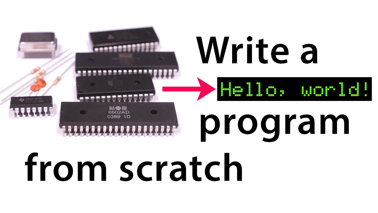
“Hello, world” from scratch on a 6502 — Part 1 — Ben Eater

Ben Eater

Hardwiring the microprocessor's floating data lines to the 0xEA NOP instruction prevents erratic executions, allowing the chip to complete its seven-cycle reset and advance sequentially through memory as a free-running counter.

AI-assisted summary of “Hello, world” from scratch on a 6502 — Part 1 — original source. Check the original for full context.

Source published:

Key ideas

  • Ben Eater initiates a bare-metal 6502 computer build to ultimately display 'Hello, world', choosing the modern static W65C02 microprocessor over vintage dynamic variants to allow single-stepping down to 0 Hz without losing internal register state. (0:00)
  • An Arduino Mega is deployed as an economical 50+ channel logic analyzer, synchronized to the 6502's clock via a hardware interrupt to sample and decode address, data, and R/W lines on every cycle. (6:55)
  • Floating data pins caused erratic execution until tied with 1 kΩ pull-up/pull-down resistors to 0xEA, providing default opcodes during reads while safely preventing short circuits during processor write cycles. (17:49)
  • Stepping through the 7-cycle hardware reset sequence reveals the processor reading the reset vector at $FFFC/$FFFD to set the program counter to $EAEA, subsequently executing NOP instructions in two clock cycles each in a classic free-run loop. (21:12)

Detailed notes

## Background Published on YouTube by Ben Eater on September 14, 2019, this video kicks off a tutorial series on computer architecture where he builds and programs a basic computer from bare silicon using the classic 6502 microprocessor. The series is designed to teach how computers work at the lowest hardware level, progressing step by step toward displaying 'Hello, world' on a physical screen.

## TL;DR Ben Eater seats a modern static W65C02 microprocessor onto a breadboard, wiring its power, control lines, and an adjustable 555-timer clock circuit. To observe the processor's internal state without an expensive logic analyzer, he configures an Arduino Mega to read the address, data, and read/write lines synchronously on rising clock edges and print formatted hexadecimal values over serial. After discovering that floating data pins cause erratic reads and writes, he uses 1 kΩ resistors to hardwire the data bus to hexadecimal $EA, the opcode for NOP (no operation). Stepping through clock pulses manually, he demonstrates the CPU's seven-cycle reset sequence, watches it fetch the reset vector from memory locations $FFFC and $FFFD, and observes the processor stabilize into a predictable free-running counter loop.

## Atmosphere & style The presentation carries the calm, methodical ambiance of a hands-on laboratory workbench, driven by Eater's clear, patient cadence and unhurried pedagogical style. The viewer experiences the tactile intimacy of wiring raw integrated circuits alongside the intellectual tension of troubleshooting erratic floating pins. When the chaotic, flickering bus output suddenly snaps into an orderly, sequential hexadecimal count, the transition delivers a quietly thrilling moment of technical satisfaction and hardware clarity.

## Bulletin - [00:00](https://www.youtube.com/watch?v=LnzuMJLZRdU&t=0s) Ben Eater initiates a bare-metal 6502 computer build to ultimately display 'Hello, world', choosing the modern static W65C02 microprocessor over vintage dynamic variants to allow single-stepping down to 0 Hz without losing internal register state. - [06:55](https://www.youtube.com/watch?v=LnzuMJLZRdU&t=415s) An Arduino Mega is deployed as an economical 50+ channel logic analyzer, synchronized to the 6502's clock via a hardware interrupt to sample and decode address, data, and R/W lines on every cycle. - [17:49](https://www.youtube.com/watch?v=LnzuMJLZRdU&t=1069s) Floating data pins caused erratic execution until tied with 1 kΩ pull-up/pull-down resistors to 0xEA, providing default opcodes during reads while safely preventing short circuits during processor write cycles. - [21:12](https://www.youtube.com/watch?v=LnzuMJLZRdU&t=1272s) Stepping through the 7-cycle hardware reset sequence reveals the processor reading the reset vector at $FFFC/$FFFD to set the program counter to $EAEA, subsequently executing NOP instructions in two clock cycles each in a classic free-run loop.

## Key takeaways - [00:00](https://www.youtube.com/watch?v=LnzuMJLZRdU&t=0s) Starting a computer from bare microprocessor hardware requires directly managing buses, clock signals, and control lines that high-level operating systems and runtimes usually abstract away. - [03:56](https://www.youtube.com/watch?v=LnzuMJLZRdU&t=236s) The project uses the modern CMOS W65C02 rather than the vintage NMOS 6502 because its static core retains register states indefinitely when the clock is stopped or slowed down. - [01:11](https://www.youtube.com/watch?v=LnzuMJLZRdU&t=71s) Active microprocessor operation requires tying control inputs like RDY, IRQB, NMIB, and BE high to prevent halting or spurious interrupt states. - [03:56](https://www.youtube.com/watch?v=LnzuMJLZRdU&t=236s) A custom 555-timer clock circuit enables variable frequency and debounced pushbutton single-stepping, which is crucial for manually observing machine cycles. - [06:55](https://www.youtube.com/watch?v=LnzuMJLZRdU&t=415s) Discrete LEDs provide immediate bus activity feedback, but quickly become impractical and visually unreadable when scaling up to monitor wide 16-bit address and 8-bit data buses simultaneously. - [06:55](https://www.youtube.com/watch?v=LnzuMJLZRdU&t=415s) The Arduino Mega acts as a cost-effective logic analyzer, offering over 50 digital I/O lines to decode and format all bus signals simultaneously over a serial connection. - [09:48](https://www.youtube.com/watch?v=LnzuMJLZRdU&t=588s) Connecting the CPU clock line to an Arduino hardware interrupt pin (pin 2) synchronizes data capture to the rising edge, preventing asynchronous read polling artifacts. - [16:18](https://www.youtube.com/watch?v=LnzuMJLZRdU&t=978s) Tracking the R/W control line is essential to determine whether data on the bus represents an instruction/operand read by the CPU or an active write operation to memory. - [17:49](https://www.youtube.com/watch?v=LnzuMJLZRdU&t=1069s) Floating bus lines act as high-impedance antennas that read random electrical noise, destabilizing the processor's internal state machine. - [19:20](https://www.youtube.com/watch?v=LnzuMJLZRdU&t=1160s) Using 1 kΩ resistors to hardwire the data bus establishes default logic levels during reads while limiting current to safe levels if the processor drives conflicting voltages during writes. - [19:20](https://www.youtube.com/watch?v=LnzuMJLZRdU&t=1160s) Hardwiring the data lines to binary 1110 1010 ($EA) stabilizes the CPU, forcing it into continuous read mode and sequential address incrementing. - [21:12](https://www.youtube.com/watch?v=LnzuMJLZRdU&t=1272s) Upon exiting reset after a seven-cycle internal initialization sequence, the 6502 fetches its starting program counter from the 16-bit reset vector at memory locations $FFFC and $FFFD. - [23:35](https://www.youtube.com/watch?v=LnzuMJLZRdU&t=1415s) The hardwired opcode $EA decodes to NOP (No Operation), which uses implied addressing and takes exactly two clock cycles per instruction to execute. - [23:35](https://www.youtube.com/watch?v=LnzuMJLZRdU&t=1415s) Continuously feeding NOP instructions creates a classic 'free-run' harness where the program counter sequentially traverses the entire 64 KB address space. - [26:02](https://www.youtube.com/watch?v=LnzuMJLZRdU&t=1562s) Building beyond the free-run verification stage requires adding programmable ROM (EEPROM) and RAM to support real software execution and peripheral display output.

## Detailed walkthrough ### [00:00](https://www.youtube.com/watch?v=LnzuMJLZRdU&t=0s) Starting from Bare Silicon: The 6502 Microprocessor

Most programming tutorials kick off by writing a trivial program that prints "Hello, world" to a terminal. While high-level languages like Python make this trivial by handling memory management, operating system calls, and display drivers under the hood, building up to that output from bare metal poses an entirely different challenge. Ben Eater introduces the central question of the build: “Well, it seems like every programming tutorial starts out having you write a simple program that just prints out hello world and it's usually a pretty simple starting point because the programming language in this case Python and everything gets built on top of does a lot of the work but what if we don't have any of that what if we just start with a microprocessor?”

The hardware at the center of the project is the classic 6502 microprocessor. Holding up a vintage chip, Eater notes its date code reveals it was manufactured in the third week of 1989, though the underlying architecture traces all the way back to 1975. Throughout the late 1970s and 1980s, variants of the 6502 powered seminal personal computers and gaming consoles like the Apple II, Commodore 64, and Nintendo Entertainment System. Despite being a 44-year-old design, brand-new versions of the chip remain in production today. Eater selects the modern static variant, the W65C02, accompanied by a concise, roughly 30-page datasheet that documents its functional pinout and electrical characteristics.

```mermaid flowchart LR accTitle: High-Level Abstraction vs Bare Hardware accDescr: Contrast between high-level Python software and bare 6502 microprocessor hardware.

subgraph SW["High-Level Abstraction"] PY["Python Print Statement"] --> OS["OS / Runtime Engine"] OS --> HW_LAYER["Display Drivers & Memory"] end

subgraph HW["Bare Metal Target"] CPU["W65C02 Microprocessor"] --> BUS["Address & Data Buses"] BUS --> SCREEN["Direct Hardware Display"] end ```

[01:11](https://www.youtube.com/watch?v=LnzuMJLZRdU&t=71s) Wiring Power, Control Lines, and Busses

Eater places the 40-pin dual in-line package (DIP) chip onto a solderless breadboard to configure its primary pins. The electrical foundation begins with the power rails: pin 8 ($V_{DD}$) connects to the $+5\text{ V}$ positive supply rail, while pin 21 ($V_{SS}$) ties to the system ground rail. However, merely providing five volts leaves the processor idle; active operation requires conditioning its dedicated input and control pins according to the datasheet specifications:

```mermaid flowchart TD accTitle: 6502 Breadboard Initial Pin Hookups accDescr: Mapping of 6502 processor pin connections to power, ground, and control logic.

subgraph Power["Power Connections"] VDD["Pin 8 (VDD)"] --> Rail5V["+5V Rail"] VSS["Pin 21 (VSS)"] --> RailGND["Ground Rail"] end

subgraph TiedHigh["Inputs Tied High (+5V)"] RDY["Pin 2 (RDY)"] --> Rail5V IRQB["Pin 4 (IRQB)"] --> Rail5V NMIB["Pin 6 (NMIB)"] --> Rail5V BE["Pin 36 (BE)"] --> Rail5V SO["Pin 38 (SO)"] --> Rail5V end

subgraph OpenOutputs["Outputs Left Unconnected"] VPB["Pin 1 (VPB)"] PHI1O["Pin 3 (PHI1O)"] MLB["Pin 5 (MLB)"] SYNC["Pin 7 (SYNC)"] PHI2O["Pin 39 (PHI2O)"] ADDR["Pins 9-20, 22-25 (A0-A15)"] end ```

- **Power**: Pin 8 ($V_{DD}$) connects to $+5\text{ V}$; Pin 21 ($V_{SS}$) connects to ground. - **Ready (RDY, Pin 2)**: An active-high input that determines whether the processor executes instructions or halts. Tied directly to $+5\text{ V}$ to keep the core running continuously. - **Interrupt Requests ($\overline{\text{IRQ}}$, Pin 4 and $\overline{\text{NMI}}$, Pin 6)**: Active-low interrupt inputs. Tied directly to $+5\text{ V}$ to prevent spurious interrupts from firing. - **Bus Enable (BE, Pin 36)**: An active-high input required for the CPU to assert signals onto both the address and data busses. Tied directly to $+5\text{ V}$. - **Set Overflow (SO, Pin 38)**: An input line intended for conditional branching hardware. The datasheet recommends tying it high when unused. - **Unconnected Outputs**: Pin 1 ($\overline{\text{VP}}$ / Vector Pull), Pin 3 ($\Phi_{1\text{O}}$), Pin 5 ($\overline{\text{ML}}$ / Memory Lock), Pin 7 ($\text{SYNC}$), Pin 39 ($\Phi_{2\text{O}}$), and Pin 35 ($\text{NC}$ / No Connect) remain open. - **Address Bus ($A_0$–$A_{15}$)**: Across pins 9–20 and 22–25, these 16 pins form the unidirectional address outputs, initially left unconnected. - **Data Bus ($D_0$–$D_7$) and Read/Write ($R/\overline{W}$)**: Data bus pins 26–33 are bidirectional. Pin 34 ($R/\overline{W}$) indicates transfer direction: logic high means the CPU is reading (data bus configured as inputs), whereas logic low signifies a memory write (data bus configured as outputs). Both are temporarily left floating.

[03:56](https://www.youtube.com/watch?v=LnzuMJLZRdU&t=236s) Clocking Architecture: Static Core vs. Dynamic Design

Any microprocessor requires a stable clock pulse to drive internal state machines and sequential execution. Original 6502 processors typically operated on a $1\text{ MHz}$ clock, whereas the modern W65C02 supports operating frequencies up to $17\text{ MHz}$. While a standard crystal oscillator module (such as a $10\text{ MHz}$ canned can oscillator) can generate clean clock inputs by simply connecting power and ground, high-speed clocks obscure internal operations from visual inspection.

Instead of a high-speed crystal, Eater utilizes a custom 555-timer-based clock module from an earlier breadboard computer build. This circuit features adjustable frequency control (allowing the user to speed up or slow down clock cycles at will), a halt toggle switch, and a debounced push button for single-stepping individual clock pulses.

Deploying this slow, single-steppable clock highlights the critical architectural distinction between the vintage NMOS 6502 and the modern CMOS W65C02. Eater explains: “And this is where it's actually really important that I'm using the modern static version of the 6502 because the datasheet here says that phi2 can be held in either the high or low state and it'll preserve the contents of internal registers and that's actually not the case with the original 6502.” Dynamic NMOS designs rely on internal capacitive charge storage that rapidly discharges if the clock speed drops below a minimum threshold (around $100\text{ kHz}$), destroying register state. In contrast, the modern W65C02 uses static logic cells that maintain their internal state indefinitely, even when the clock input at Pin 37 ($\Phi_2$) is held completely stationary in either a logic high or logic low state.

To control startup, Pin 40 ($\overline{\text{RES}}$ / Reset) requires active pull-up conditioning. Eater attaches a $1\text{ k}\Omega$ pull-up resistor from Pin 40 to $+5\text{ V}$, holding the processor in operational mode during normal conditions. A momentary tactile push button is wired between Pin 40 and ground; pressing the switch shunts Pin 40 directly to ground, asserting a hard hardware reset.

```mermaid flowchart LR accTitle: Reset and Clock Input Circuits accDescr: Schematic implementation of the 555-timer clock input and manual reset switch.

subgraph ClockGen["Clock Subsystem"] TMR["555 Timer Module"] -->|"Variable / Step"| PHI2["Pin 37 (PHI2)"] end

subgraph ResetCirc["Reset Subsystem"] VCC["+5V"] --- R1["1k Resistor"] R1 --- RES["Pin 40 (RES)"] SW["Push Button"] --- RES SW --- GND["Ground"] end ```

[06:55](https://www.youtube.com/watch?v=LnzuMJLZRdU&t=415s) Diagnosing Activity: LEDs vs. Logic Analyzers vs. Arduino

With $+5\text{ V}$ power supplied, the variable clock running, and the manual reset button cycled, the processor begins stepping through its internal startup sequence. However, with the address and data busses floating in midair, there is no immediate visual indication of what the microprocessor is doing. To observe pin activity, Eater installs five discrete LEDs on the breadboard, wiring their anodes to address lines $A_0$ through $A_4$ and their cathodes to ground through current-limiting $220\ \Omega$ resistors.

Pulsing the clock produces flickering light patterns across the five LEDs, confirming that internal state changes are toggling the bus pins. However, monitoring only five bits provides an incomplete, cryptic picture. Monitoring all sixteen address lines, eight data bus lines, and multiple control pins simultaneously would require dozens of LEDs, cluttering the breadboard and making chronological analysis virtually impossible to track by eye.

```mermaid flowchart TD accTitle: Diagnostic Tool Tradeoffs accDescr: Comparison of breadboard diagnostic methods highlighting the Arduino Mega.

LED["Breadboard LEDs"] -->|"Pros: Simple\nCons: Limited pins, hard to read"| LIMIT1["Poor Visibility"] LA["Hardware Logic Analyzer"] -->|"Pros: MHz sampling, waveforms\nCons: Only 16 channels, overkill for slow clock"| LIMIT2["Channel Constrained"] ARD["Arduino Mega 2560"] -->|"Pros: 50+ digital I/O, cheap, direct decode\nCons: Low sample rate (acceptable here)"| BEST["Optimal Monitoring Tool"] ```

While a dedicated 16-channel logic analyzer excels at capturing high-frequency digital waveforms over time, Eater points out that it presents practical limitations for this setup: it is channel-constrained, and its high sampling rates are unnecessary when single-stepping or running the clock at sub-kilohertz speeds. Eater argues for a simpler approach: “I think a much better and definitely less expensive tool is actually just an Arduino because if we want to monitor what these address lines are doing we could just hook them up to inputs on the Arduino and have the Arduino just read whatever is on each of these pins and you know, especially something like this Arduino Mega it's got, you know, something like 50 digital inputs so way more than the 16 inputs that we have on nice logic analyzer like this.” The Arduino Mega can sample all address lines, data lines, and control signals on every clock pulse, formatting and printing the machine state directly to a serial terminal.

[09:04](https://www.youtube.com/watch?v=LnzuMJLZRdU&t=544s) Connecting the Address Bus to an Arduino Mega

Ben Eater decides to clear away the bulky logic analyzer probes and the breadboard LEDs to replace them with an Arduino Mega. Because the 6502 microprocessor has a 16-bit address bus, an Arduino Mega provides more than enough general-purpose digital I/O pins to monitor every address line simultaneously. He attaches a 16-conductor ribbon cable running from the processor's address pins (A0 through A15) straight into a bank of Arduino digital inputs, remembering to connect a common ground between the two boards. Ben Eater summarizes the setup: “So just like the logic analyzer the Arduino can then keep track of you know, what each address line is doing.”

```mermaid flowchart LR accTitle: Arduino Mega Bus Monitor Setup accDescr: Diagram showing the 6502 address and clock lines hooked up to the digital pins of an Arduino Mega. subgraph CPU["W65C02 Microprocessor"] A["Address Lines (A15–A0)"] CLK["Clock Line (PHI2)"] end subgraph Arduino["Arduino Mega"] D_PINS["Pins 22–52 (Even)"] INT_PIN["Pin 2 (Interrupt)"] UART["Serial Monitor (57,600 baud)"] end A -->|"16-pin ribbon cable"| D_PINS CLK -->|"Interrupt trigger"| INT_PIN D_PINS --> UART INT_PIN --> UART ```

In the Arduino IDE, Ben writes a sketch defining the specific pins used for the address bus, starting with address bit A15 mapped to pin 22 and descending through the even-numbered header pins down to A0 on pin 52. In the `setup()` function, a `for` loop iterates through all 16 pins to configure their `pinMode` as `INPUT`, while initializing serial communication at a standard baud rate of 57,600. In the `loop()` function, the code reads each pin in order with `digitalRead()`, checks whether the boolean returned is true or false to print a literal `1` or `0` to the serial monitor, and appends a newline after printing all sixteen bits.

- Address line mapping: Pin 22 (A15) down through pin 52 (A0). - Serial speed: Configured to 57,600 baud. - Initial read implementation: Continuous polling inside `loop()`, spitting raw 16-bit binary strings across the terminal.

[09:48](https://www.youtube.com/watch?v=LnzuMJLZRdU&t=588s) Reading the Bus and Adding Clock Synchronization

When Ben uploads the sketch and opens the serial monitor, binary numbers immediately begin streaming across the screen. However, interpreting this raw stream proves difficult because the values scroll uncontrollably. Ben notes: “It looks like it's just kind of spewing a bunch of ones and zeros that are changing, you know maybe on every clock pulse, or maybe it's every other clock pulse.” Because the Arduino's `loop()` runs asynchronously at its own processing rate, it reads the address pins at random intervals relative to the 6502's clock cycles, making it impossible to correlate bus states with specific instructions.

To fix this, Ben takes advantage of the Arduino's remaining digital I/O pins by routing the 6502 clock signal to digital pin 2. Digital pin 2 on the ATmega board supports hardware interrupts. Rather than reading the clock inside the standard loop, Ben invokes `attachInterrupt()` in `setup()` to bind an interrupt handler function named `onClock` to pin 2, configuring it to trigger specifically on the rising edge (`RISING`) when the clock transitions from low to high.

Ben empties out `loop()` entirely and migrates the bus-reading code into `onClock()`. Ben explains the reasoning: “The only time we do anything is when we get a clock pulse and then we just print the address once so let's give this a try.” When the updated sketch runs, the serial monitor prints exactly one line of data per clock pulse. Halting the clock module cleanly freezes the serial output, allowing Ben to pulse the clock manually and single-step through cycles one by one.

- Clock input: Connected directly to Arduino digital pin 2. - Interrupt trigger: Configured for the rising edge of the clock signal (`RISING`). - Behavior: The Arduino loop does nothing; bus state is printed strictly once per clock tick, enabling precise manual single-stepping.

[13:23](https://www.youtube.com/watch?v=LnzuMJLZRdU&t=803s) Monitoring the Data Bus and Formatting Hex Output

While stepping through single cycles provides stable readings, raw 16-bit binary remains tedious to decipher. To understand what the processor is actually attempting to execute, Ben decides to inspect the 8-bit data bus (D7 down to D0) alongside the address bus. He connects eight additional jumper wires from the processor's data lines to pins 39 through 53 (the odd-numbered pins) on the Arduino Mega header, then declares these pins in the sketch and sets their `pinMode` to `INPUT` during setup.

```mermaid flowchart TD accTitle: Bus Processing and Formatting Flow accDescr: Flowchart illustrating how address and data pins are read, bit-shifted into numerical values, and formatted as hex. Start["Rising Clock Edge (onClock Interrupt)"] --> ReadAddr["Read Pins 22–52 (16 bits)"] ReadAddr --> ShiftAddr["Shift Left & Accumulate into 16-bit unsigned int"] ShiftAddr --> ReadData["Read Pins 39–53 (8 bits)"] ReadData --> ShiftData["Shift Left & Accumulate into 8-bit unsigned int"] ShiftData --> ReadRW["Read Pin 3 (R/W Line)"] ReadRW --> Format["sprintf(output, '%04x %c %02x', addr, r_w, data)"] Format --> Print["Serial.println(output)"] ```

Ben also addresses the readability of the bus values. Ben Eater remarks: “The other thing I can do here to make it easier to sort of interpret what's going on is instead of just printing out the binary ones and zeros like we are we could print the values in decimal or actually in hexadecimal.” Instead of printing characters directly during the bit-reading loops, he initializes an unsigned integer variable to zero, shifts it left by one bit on every iteration (`address = (address << 1) + bit`), and adds the current bit. By repeating this pattern for both the 16 address bits and the 8 data bits, he converts the bus signals into clean numeric values.

Using `sprintf()`, Ben formats the accumulated values into a 15-character buffer, displaying the address as a 4-digit hexadecimal number (`%04x`) and the data as a 2-digit hexadecimal number (`%02x`).

- Data bus mapping: Pins 39 through 53 (odd numbers) monitor D7 down through D0. - Numerical conversion: Bit-shifting accumulation converts 16 address bits into an unsigned 16-bit integer and 8 data bits into an unsigned byte. - String output: `sprintf` formats the values into a compact hex readout.

[16:18](https://www.youtube.com/watch?v=LnzuMJLZRdU&t=978s) Tracking the Read/Write Signal and Interpreting Bus Traffic

Ben points out that knowing the address and data values is still not enough to understand the processor's intent because the data bus is bidirectional. He introduces the processor's Read/Write ($R/\bar{W}$) control signal. Ben Eater explains how it operates: “So this read/write pin is high then it means the processor is reading from the data bus and if this is low then it means it's writing to the data bus.” Tracking this line is essential for determining whether the CPU expects external memory to supply an opcode or operand, or whether the CPU is driving data out to store it.

Ben connects the $R/\bar{W}$ pin to digital pin 3 on the Arduino, defines it in code, and sets it as an input in `setup()`. In `onClock()`, the sketch performs a `digitalRead()` on pin 3 and adds an indicator character to the serial output string: printing an `r` when the line is high (reading) and a `W` when the line is low (writing). After catching a minor syntax error—a missing comma in his `sprintf()` arguments—Ben re-uploads the sketch and starts the clock.

``` Expected Serial Output Format: [Address (hex)] [R/W] [Data (hex)] 04a2 r ea 04a3 r ea 01fd W 04 ```

The serial monitor springs to life with formatted output displaying addresses, read/write states, and data values. Even with this clean format, the processor's behavior appears chaotic: addresses leap across the memory map unpredictably, data values fluctuate wildly, and the chip alternates erratically between read and write cycles.

- $R/\bar{W}$ line mapping: Routed to Arduino pin 3. - Output notation: `r` indicates the processor is reading data; `W` indicates the processor is writing data.

[17:49](https://www.youtube.com/watch?v=LnzuMJLZRdU&t=1069s) Floating Inputs and Tying the Data Bus with Resistors

Ben analyzes why the processor behaves so erratically despite the monitoring code functioning properly. He points out that while the Arduino is reading the data lines, nothing on the breadboard is actually driving them during read cycles. The data bus pins are floating, disconnected from any memory chip or peripheral. Whenever the 6502 flags an `r` cycle to read an instruction byte from memory, it reads electrical noise and floating capacitance. Ben Eater observes: “So if the processor is just kind of reading garbage whenever it reads from those data pins, you know I guess I would sort of expect it to behave kind of randomly.”

To establish predictable behavior without wiring in a full ROM chip yet, Ben decides to hardwire the data pins to a known, constant bit pattern. To do this safely, he ties each of the eight data pins to either +5 volts (logic high) or ground (logic low) using 1 kΩ current-limiting resistors rather than direct wire jumpers.

The 1 kΩ resistors serve an important electrical purpose: when the 6502 is reading, the processor's high-impedance inputs easily read the weak logic levels pulled through the resistors as valid ones and zeros. However, when the 6502 occasionally enters a write state (`W`) and actively drives its own output voltages onto the data bus, the processor's internal drivers easily override the weak resistor pulls without causing a short circuit between power and ground.

- Cause of errant execution: The data bus is floating, feeding random garbage opcodes to the CPU during read cycles. - Temporary solution: Hardwire each data bus line to a fixed logic level (5V or GND) via 1 kΩ resistors. - Electrical protection: 1 kΩ series resistors provide a default logic level during CPU reads, while allowing the CPU's active output drivers to override the line safely during write cycles without drawing excessive current.

[19:20](https://www.youtube.com/watch?v=LnzuMJLZRdU&t=1160s) Hardwiring an Opcode: Setting Up 0xEA on the Data Bus

To prevent the processor from driving illegal states or floating into erratic behavior, Ben connects a series of resistors to the data bus pins. In the worst-case scenario where the processor outputs an opposite logic level, there would only be a five-volt potential difference across each resistor, safely limiting current. As Ben explains: “In other words these resistors that I'm putting that I'm adding here are just kind of setting a default value, but you know if the processor outputs something different then you know, no big deal.” He ties each resistor to either ground or 5 volts in a specific pattern, presenting the binary value `1110 1010`—hexadecimal `$EA`—to the data bus pins.

```mermaid flowchart TD accTitle: 6502 Reset and Free-Run Execution Flow accDescr: Flowchart showing how the 6502 initializes across seven cycles, fetches the reset vector from memory, and repeatedly executes NOP instructions.

subgraph ResetPhase ["Hardware Reset"] R1["Reset line pulsed low"] --> R2["Internal reset sequence<br/>(7 clock cycles)"] end

subgraph VectorFetch ["Reset Vector Fetch"] R2 --> V1["Read low byte from $FFFC<br/>(Gets $EA)"] V1 --> V2["Read high byte from $FFFD<br/>(Gets $EA)"] V2 --> V3["Load Program Counter<br/>PC = $EAEA"] end

subgraph Execution ["Execution Loop"] V3 --> E1["Fetch opcode at PC ($EAEA)<br/>(Reads $EA / NOP)"] E1 --> E2["Execute NOP<br/>(Takes 2 clock cycles)"] E2 --> E3["Increment PC<br/>PC = PC + 1"] E3 --> E1 end ```

Once the bus is tied off and powered up, the processor’s erratic output vanishes immediately. The Arduino serial monitor shows that the 6502 is now exclusively performing read operations rather than alternating unpredictably between reads and writes. On every read cycle, the data byte returned is `$EA`. Furthermore, the address bus stops jumping randomly across the address space and begins incrementing sequentially: `... FFFE, FFFF, 0000, 0001, 0002...` through memory in an orderly hexadecimal progression. Simply establishing a steady, predictable input on the data bus stabilizes the processor's internal state machine.

- The hardwired data bus pattern is binary `1110 1010`, corresponding to hexadecimal `$EA`. - The pull-up and pull-down resistors act as default bus terminators without short-circuiting outputs if the processor drives the bus. - With data lines defined, the read/write line (`R/W`) stays high (read mode) instead of thrashing, and the address bus behaves as a continuous sequential counter.

---

[21:12](https://www.youtube.com/watch?v=LnzuMJLZRdU&t=1272s) Stepping Through the Reset Sequence and the Reset Vector

When Ben pushes the onboard reset button, the address bus momentarily shifts before settling back into its counting routine. Consulting the Western Design Center W65C02S datasheet, he reviews the exact behavior of the reset pin: “It says when a positive edge is detected, there'll be a reset sequence lasting seven clock cycles.” To observe this directly, Ben holds down the reset switch, halts the automated clock module, clears the Arduino serial monitor, and manually single-steps the clock using the pushbutton.

Advancing the clock seven single pulses completes the seven internal reset cycles, during which the processor carries out housekeeping tasks. On the eighth clock cycle, the chip places address `$FFFC` onto the address bus and signals a read. The datasheet specifies that upon exiting reset, the program counter register is populated from the 16-bit reset vector located at addresses `$FFFC` (holding the low byte) and `$FFFD` (holding the high byte). Advancing the clock once more places `$FFFD` on the address bus. Because Ben has hardwired the data lines to `$EA`, the CPU reads `$EA` for the low byte at `$FFFC` and another `$EA` for the high byte at `$FFFD`. Consequently, the internal program counter is loaded with the start address `$EAEA`.

- Reset initialization on the 6502 requires exactly seven clock cycles following a positive edge. - Memory locations `$FFFC` and `$FFFD` form the 16-bit reset vector defining the execution entry point. - Because the hardwired bus returns `$EA` on every access, the processor loads the low byte `$EA` and high byte `$EA`, setting `PC = $EAEA`.

---

[23:35](https://www.youtube.com/watch?v=LnzuMJLZRdU&t=1415s) Fetching and Executing NOP: The Free-Running Counter

With the reset vector loaded, the processor is primed to begin fetching instructions. Stepping the clock one additional cycle reveals that the address lines immediately update to `$EAEA`, exactly matching the loaded program counter value. The processor outputs a read request to fetch its first instruction from this location and reads `$EA` from the bus resistors. It must now decode and execute `$EA`.

Ben looks up `$EA` in the datasheet's opcode matrix: locating row `E` and column `A` reveals that `$EA` corresponds to the `NOP` instruction—"no operation." As Ben observes: “So basically the processor is going to do nothing.” Stepping the clock again increments the address to `$EAEB`, where the CPU reads another `$EA`, executing another `NOP`. He notes an important architectural timing detail: it takes two full clock cycles for each address increment to occur. Cross-referencing the datasheet's opcode matrix reveals a small subscript `i` next to `NOP`, denoting the implied addressing mode. The addressing mode specification confirms that instructions utilizing implied addressing require two clock cycles to complete. Running the clock continuously produces a classic "free-run" harness where the CPU loops forever, taking two clock cycles per instruction to do nothing while steadily counting across the entire 64 KB address space.

- Opcode `$EA` decodes to `NOP` (No Operation) on the 6502 microprocessor. - `NOP` uses implied addressing (marked by an `i` in the matrix) and requires exactly two clock cycles per instruction execution. - In this open-bus state, the CPU operates as an automated 16-bit counter, incrementing its program counter across memory without branching or halting.

---

[26:02](https://www.youtube.com/watch?v=LnzuMJLZRdU&t=1562s) Looking Ahead: Kits, EEPROMs, and Future Plans

While hardwiring the data bus proves that the microprocessor can reset, fetch, decode, and execute instructions, Ben points out that a machine forced to execute nothing but hardwired `NOP`s is not yet a functional computer. In the upcoming video, he plans to replace the resistor network with a programmable ROM chip so that the processor can fetch real instructions from distinct memory addresses, paving the way toward a functional "Hello, World" program.

Ben announces that he has assembled a full hardware kit for viewers wanting to build along with the project, available through his website at `eater.net/6502`. The kit includes the 6502 CPU along with RAM, ROM, an LCD screen, and input buttons, leading toward building an interactive assembly language game. He emphasizes that builders will also need an external EEPROM programmer, along with the 555-timer clock module kit and the Arduino Mega used as the diagnostic bus monitor. He closes by thanking the Patreon supporters whose contributions fund these hardware build projects.

- The next stage replaces hardwired resistors with an EEPROM chip containing programmed software routines. - The project kit at `eater.net/6502` includes the 6502 microprocessor, RAM, ROM, and I/O components intended to support a display and an assembly language game. - Essential complementary tools not included in the primary chip kit comprise a dedicated EEPROM programmer, the custom 555-based clock module, and an Arduino Mega logic monitor.

## Mentioned Ben Eater, 6502 microprocessor, W65C02, Apple II, Commodore 64, Nintendo Entertainment System, Arduino Mega, Arduino IDE, 555 timer, Python, Western Design Center, Patreon

## Video description Learn how computers work in this series where I build and program a basic computer with the classic 6502 microprocessor. More info: https://www.eater.net/6502

Part 2: https://www.youtube.com/watch?v=yl8vPW5hydQ Part 3: https://www.youtube.com/watch?v=oO8_2JJV0B4 Part 4: https://www.youtube.com/watch?v=FY3zTUaykVo Part 5: https://www.youtube.com/watch?v=xBjQVxVxOxc Part 6: https://www.youtube.com/watch?v=i_wrxBdXTgM Part 7: https://www.youtube.com/watch?v=omI0MrTWiMU

Support these videos on Patreon: https://www.patreon.com/beneater or https://eater.net/support for other ways to support.

------------------

Social media: Website: https://www.eater.net Twitter: https://x.com/beneater Patreon: https://patreon.com/beneater Reddit: https://www.reddit.com/r/beneater

Special thanks to these supporters for making this video possible: Alex Catchpole Armin Brauns BakerStaunch Beau-James Erion Ben Ben Dyson Ben Kamens Ben Williams Bradley Pirtle Christopher Blackmon Clayton Parker Coleman Daniel Tang Dean Winger Debilu Krastas Dominic Kulmer Dušan Dželebdžić Eric Brummer Eric Dynowski Erik Broeders Eugene Bulkin fxshlein HaykH Ian Tait Ivan Sorokin JavaXP Jay Binks Jayne Gabriele Jefferson Hunt Jimmy Campbell Joel Messerli Joel Miller Jordan Scales Joshua King Justin Duch Kent Collins Manne Moquist Marcus Classon Mats Fredriksson Michael Michael Burke Michael Garland Miguel Ríos Nathan Wachholz Nicholas Moresco Onion Sniffer Paul Pluzhnikov Peter Simard Randy True Robert Butler Sachin Chitale Sergey Ten SonOfSofaman Stefan Nesinger Stephen Smithstone Steve Gorman Thomas Ballinger Vladimir Kanazir xisente Örn Arnarson

[Source](https://www.youtube.com/watch?v=LnzuMJLZRdU)

Reading summary

Ben Eater demonstrates how to bring up a bare-metal 6502 microprocessor on a solderless breadboard, validating its fundamental execution cycles before integrating memory or software. By interfacing the chip with an Arduino Mega bus monitor and hardwiring the data bus to a fixed instruction, he confirms the processor's reset sequence and internal state machine. Hardware Wiring and Static Clocking Advantages (1:11) Eater configures a modern CMOS W65C02 microprocessor on a solderless breadboard, supplying +5 V to pin 8 (VDD) and ground to pin 21 (VSS). Essential control inputs—including Ready (RDY), Interrupt Requests (IRQ and NMI), Bus Enable (BE), and Set Overflow (SO)—are tied directly to +5 V to ensure continuous operation and prevent spurious interrupts. A 1 kΩ pull-up resistor and a momentary pushbutton wired to ground on pin 40 (RES) provide a manual hardware reset switch. Eater highlights a vital architectural distinction in selecting the modern static W65C02 over vintage NMOS designs. Original dynamic 6502 chips rely on internal capacitive charge storage that degrades if the clock drops below roughly 100 kHz, causing register corruption. The static CMOS core, however, can hold its clock input (PHI2, pin 37) high or low indefinitely without losing state. This allows Eater to replace high-speed crystal oscillators with an adjustable 555-timer module capable of single-stepping individual clock cycles for manual inspection. Constructing an Interrupt-Driven Bus Monitor (9:04) To monitor bus activity without overwhelming the breadboard with LEDs or using a channel-constrained logic analyzer, Eater connects the CPU to an Arduino Mega. A ribbon cable links the 16 address lines (A0–A15) to Arduino pins 52 through 22, eight data lines (D0–D7) to pins 53 through 39, and the Read/Write (R/W) line to pin 3. Because continuous polling in the Arduino's main loop generated an unsynchronized stream of bus readings, Eater routes the 6502 clock signal to Arduino digital pin 2 and binds an interrupt service routine to its rising clock edge. The Arduino reads the pins precisely once per clock cycle, assembling the binary inputs into numeric variables via bit shifting. Using sprintf(), it prints a clean serial record showing the 4-digit hexadecimal address, whether the operation is a read ('r') or write ('W'), and the 2-digit hexadecimal data byte. Stabilizing Floating Inputs with Resistor Termination (17:49) Initial tests produced erratic bus activity, with addresses jumping unpredictably across the memory map and the processor thrashing between read and write states. Eater identifies the cause: with no external memory wired, the bidirectional data bus floats during read cycles, causing the CPU to ingest ambient electrical noise and floating capacitance as random instructions. To establish predictable behavior without wiring in a ROM chip, Eater connects each of the eight data pins to either +5 V or ground using 1 kΩ current-limiting resistors, forcing a constant binary pattern of 1110 1010 (hexadecimal $EA). The 1 kΩ resistors provide essential electrical safety: during read cycles, the CPU's high-impedance inputs easily read the weak pull-up or pull-down voltages, while any write cycle allows the CPU's active output drivers to override the resistor pulls without creating a destructive short circuit between power and ground. Validating the Reset Sequence and NOP Execution (21:12) Terminating the data bus immediately stabilizes the processor into read mode and allows direct observation of its startup sequence. Consulting the WDC datasheet, Eater notes that detecting a positive edge on the reset line triggers an internal reset sequence lasting seven clock cycles. On clock cycles eight and nine, the processor accesses the 16-bit reset vector at addresses $FFFC (low byte) and $FFFD (high byte). Because the hardwired data bus returns $EA on every cycle, the CPU loads low byte $EA and high byte $EA, setting the program counter to $EAEA. On the tenth clock cycle, the CPU begins program execution by reading address $EAEA, fetching opcode $EA. In the 6502 architecture, $EA corresponds to the NOP (No Operation) instruction under implied addressing. The datasheet specifies that implied addressing instructions require two clock cycles to complete. With the clock running continuously, the CPU advances across all 64 KB of memory two clock cycles per step, creating a free-running 16-bit counter. Hardwiring a continuous NOP loop confirms that the CPU can reliably reset, fetch, and execute instructions, but Eater emphasizes that the system remains an open counter rather than a true computer. Building toward a functional 'Hello, world' program requires replacing the resistor network with an EEPROM containing executable software, accompanied by RAM and an output display.

Original transcript

[0:00] Well, it seems like every programming tutorial starts out having you write a simple program that just prints out hello world [0:05] and it's usually a pretty simple starting point because the programming language in this case Python and everything gets built on top of [0:11] Does a lot of the work but what if we don't have any of that what if we just start with a microprocessor? [0:16] And how do we get from this to printing HelloWorld on a screen of some sort? [0:21] Well, this is the 6502 microprocessor and it's a real classic [0:25] You can see from the date code that this one was manufactured in the third week of 1989 [0:29] but the design for this has been around since [0:32] 1975 and versions of this chip found their way into many personal computers and game consoles in the 80s [0:37] But believe it or not [0:38] Even though the original design is 44 years old a version of the 6502 is still being manufactured today [0:44] And in fact for reasons, I'll get into later. I'm gonna use this modern version [0:48] and so here it is and here's the datasheet Ford and you can see the data sheets only about 30 pages long, but well [0:54] Let's start take a look at the pinout for this and start hooking up some of these pins to see what we can get it [0:59] To do you can see there's a description here as well [1:01] For what each of the pins are and if we flip back a couple pages [1:05] You can see a more detailed description of each of the pins and exactly what the function is [1:11] But let's start with the power pin. So VDD is positive power VSS is the ground [1:16] so I'll put the microprocessor on a breadboard here and [1:19] VDD is pin eight and that's our positive power supply [1:22] So I'll connect that to the positive power rail of our breadboard and then VSS is pin 21, so that's ground [1:28] So I'll connect that to the ground rail on the breadboard [1:30] So at this point if we connected five volts here to our breadboard it would power up the microprocessor [1:35] but it's not gonna do very much because we need to connect some of these other pins and if we look at these pins you [1:40] Know some are going to be inputs and some are going to be outputs and the outputs [1:43] I'm not gonna worry about too much just yet. Yes, for example [1:46] Pin 1 here is vector pol and we can see here that is an output and it indicates, you know some particular condition [1:51] But if we don't care about what it's outputting then we don't need to connect it to anything to get the processor to work [1:56] Yeah, but that's not the case for pin 2 your pin 2 is the ready pin and that's it [2:00] And you can see that's an input and so it is going to matter to the processor what we hook this to and in fact [2:04] the ready signal indicates [2:06] so whether the processor is going to run or orbit or halt and [2:09] So if we want it to run we need to hook pin 2 to 5 volts [2:12] It's now I'm basically going to do same thing for the rest of these pins, you know any pins that are inputs [2:17] I want to hook to something reasonable. That'll get the microprocessor to run and so I'll just go pin by pin [2:22] So pin three here five 100. That's an output [2:25] So I'm not gonna worry about that [2:26] Pin four is the IR QB that's interrupt request and that that's an input and bringing it low will trigger an interrupt [2:33] So I'll just high it high for now so that we're not triggering an interrupt [2:36] Pin five MLB that's a memory lock. That's another output. So I'll leave that alone and it might be that's the non-maskable interrupt [2:43] So just like the regular interrupt request here [2:46] Bringing it low triggers the non-maskable interrupt. So I'll tie that high as well [2:49] So we're not triggering that sync is another output. So we'll connect that to anything yet VDD, of course. We already have that connected [2:55] that's our positive power supply and then we have this a zero all the way around through a [2:59] 15 and these are the sixteen address lines and so they're actually all outputs [3:04] So I'll leave them unconnected for now as well in the mix. We have these these eight pins here d0 through d7 [3:10] That's the the data bus and these can actually be inputs or outputs [3:14] and in fact the next pin here this rwb pin 34 [3:17] That's an output signal that tells us whether the processor is using the data pins for input or for output [3:22] So this read/write signal and on pin 44 34 if that's high then that means the data bus pins are inputs [3:28] And if that's low then it means the data bus pins are our outputs [3:31] So for now I'm going to leave these unconnected, but we will need to come back here and connect something to these [3:36] So moving on NC is no connect. So that means we actually shouldn't connect anything to that. So that's easy [3:42] In 36b II that's bus enable and that's another input [3:46] so the bus enable signal needs to be high in order for the processor to put anything out on either the address bus or the [3:51] Data bus. So basically we want that to be high all the time. So I'll connect pin 36 to 5 volts [3:56] So it's high and then we get to pin 37 is phi2 and that's the clock input and you know [4:02] Like all computers. We need a system clock in order to provide timing toward the microprocessor and [4:07] You know the original 6502 used a 1 megahertz clock [4:11] But this modern version that I'm using is a bit more flexible so we can actually run it up to 17 megahertz [4:16] You know an easy way to provide a clock input is to use one of these crystal oscillator modules, you know [4:21] This one for example is 10 megahertz [4:22] And so if we just connected ground and 5 volts here [4:25] It would output a 10 megahertz clock that could then just connect directly to pin 37 up here [4:30] But in this video, I actually want to run the clock much slower so we can really see what's going on [4:34] So I'm not going to use this instead [4:36] I'm going to use this clock module that I built in some previous videos for for my other breadboard CPU project and [4:42] If I power this up you can see us it gives us a clock pulse that we can actually adjust [4:46] So I can slow it down [4:48] or speed it up and and we can also halt it and [4:51] Then single-step it so we can get nice single clean clock pulses that way [4:56] And if you want to know more about how this works, you know [4:58] I've got several videos that walk through it all and [5:00] explain how the the five five five timer that we're using works in a stable monostable and by stable modes, so [5:06] You know check that out there [5:07] If you're if you're interested there in any event, I'll connect this clock here to pin 37 [5:13] which is our clock input over here and [5:15] Let that clock run and this is where it's actually really important that I'm using the modern static version of the 6502 [5:22] Because the datasheet here says that phi2 can be held in either the high or low state and it'll preserve the contents of internal registers [5:29] And that's actually not the case with the original 6502 [5:32] If the clock for this stopped or got too slow, it just wouldn't work [5:36] You'd lose the contents of the internal registers [5:39] But but here because we're using this this modern the W 65 c02 which is a fully static design [5:45] We can stop the clock and we can single-step it which is which is really nice [5:49] and so that's the clock pin 37 and so just for the last couple of pins pin 38 is set overflow and [5:55] that that's an input but the datasheet basically says it's not recommended to do anything with it other than just high and high so so [6:01] that's what I'll do and [6:02] Then pin 39 5 - oh, that's an output [6:05] So we won't do anything with that and then pin 40 is the reset signal which normally needs to be tied high when the processor [6:11] Is running but will want to be able to bring it low to reset the processor [6:14] So what I'll do is I'll tie it high through a 1k resistor [6:18] So now it's tied to 5 volts through that 1k resistor [6:21] But then what I'll do is I'll add a button here and then I'll connect the other side of the button to ground that way [6:26] When we push the button that will short this pin to ground and and and trigger a reset [6:31] Otherwise if we're not pushing the button it won't be shorted to ground and it will be tied to 5 volts through that resistor [6:35] And so that ought to take care of pretty much everything [6:37] We need to set up just to get the processor to do something. And so I've connected power across here [6:42] So if we just plug in five volts over here, then that should power up everything and of course [6:47] We've got the clock running. So we hit the reset button here. That should reset the microprocessor [6:52] And now the processor is is maybe doing something [6:55] But but what is it doing? How can we figure out what's going on here? [6:59] Well, you know, of course [6:59] We still have a bunch of output pins here that we haven't hooked anything yet [7:02] So we could hook up some of those output pins, you know to drive some LEDs and see if they're doing anything [7:08] So let's give that a try [7:09] I'll add a couple LEDs here that we can use to look at some of the outputs from the microprocessor and [7:14] Then I'll connect a few of the address lines to them [7:17] And so I'm just connecting up the first five address lines a zero through a four [7:21] And then I'll connect the other side of the LEDs to ground through 220. Ohm resistors and okay, so [7:29] something's going on here, you know the process is doing something but you know, I'm not really entirely sure what so [7:36] How can we get a better picture of what's going on here? [7:38] you know well [7:39] We could certainly add a bunch more LEDs to look at the rest of the address lines and maybe look at some of the data [7:43] lines and maybe some of these other output signals, but you know [7:46] That's that's a lot of LEDs and it's gonna be really hard to keep track of everything going on, you know [7:50] Especially if we're trying to sort of figure out kind of a pattern over over a period of time [7:54] Yeah, but there are tools we can use to make analyzing a digital circuit like this easier [7:58] So, for example, we could use a logic analyzer which has a whole bunch of inputs [8:02] and you know [8:02] the one I've got has 16 inputs here and we can hook each of these inputs up to a separate signal and [8:08] use the logic analyzer to capture what's going on over a period of time so we can analyze it and [8:12] Then if we capture while the circuit is running what we get is a display like this that tracks each of the signals [8:18] So here we can see all of our address lines and you know, maybe you try to figure out from this, you know [8:22] What's going on? [8:23] And so logic analyzer is great, especially for a high-speed circuit with a lot going on [8:27] But for something lower speed like this that we can actually run and we in fact want to run pretty slow [8:32] Yeah, I think a logic analyzers is overkill, you know [8:35] I think I'm much better and definitely less expensive tool is actually just in Arduino [8:40] because if we want to monitor what these address lines are doing [8:42] we could just hook them up to inputs on the Arduino and have the Arduino just read whatever is on each of these pins and [8:47] You know, especially something like this Arduino mega. It's got, you know, something like 50 digital inputs [8:52] So way more than the 16 inputs that we have on [8:55] Nice logic analyzer like this the drawback, of course is you know, the Arduino is much slower, you know [8:59] We can read millions of samples per second with a logic analyzer. But that's fine, you know for running our clocks slow enough [9:04] That's that's not going to be a big deal [9:07] So forget the logic analyzer out of the way and also get these LEDs out of here [9:11] Then what I can do is hook those 16 address lines up to 16 of the digital i/o pins on this Arduino, you know [9:17] So just like the logic analyzer the Arduino can then keep track of you know, what each address line is doing [9:22] so I'll connect this ribbon cable with 16 connectors over to 16 of the digital inputs on the Arduino and [9:30] On the other end. I'll connect to the 16 address lines [9:34] And also need to connect the ground [9:36] Of course and so once I've got the 16 address lines then connected into 16 digital i/o pins of the Arduino [9:42] I don't need to program the Arduino to read each other's address lines and show us what it's doing [9:48] Okay [9:48] So I'll start by listing out the 16 pin numbers that I used and I guess I could use any of the digital i/o pins [9:53] on the Arduino [9:54] But these are the 16 pins that I used for the address [9:57] Starting with a 15 which is on pin 22 [9:59] And going to a 0 which is on pin 52 at the bottom then in the setup function. I'll loop through all 16 pins and [10:06] Set the pin mode for each 2 [10:08] Input and so what that does is just sets all 16 of these pin numbers here [10:12] It just it just goes through all 16 of them and sets them to input and then in the loop function here [10:17] I want to I want to go through each of those same pins again [10:21] And here I want to actually read each bit. I [10:25] think digital read returns a boolean [10:27] So if I want a 1 or a 0 here and I can say if it's true, I want a 1 [10:31] otherwise I want to 0 and [10:33] then what I can do is I can assign this to an integer and then after we have that 0 or 1 we can we [10:38] Can print that to the serial monitor? [10:40] Then after we've printed all 16 bits here, then we'll print a new line. So this ought to read all 16 bits [10:46] From from pin 22 which is which is address 15 all the way down to address 0 and print each bit in order [10:53] And then print a new line. It'll just keep doing that [10:56] And of course in our setup, we need to initialize the serial port up here. So we'll initialize the serial port to [11:01] 57600 which is just a standard speed. Okay. So this oughta continually read those 16 bits and print them on the serial [11:09] So let's give it a try. I'll connect the Arduino up and then compile and upload the sketch [11:16] There we go now if I open up the serial monitor [11:22] Hey we are seeing [11:24] Or saying some numbers and so it looks like we're getting what we're getting something. But how do we make sense of this? [11:30] You know, it looks like it's just kind of spewing a bunch of ones and zeros that are changing, you know [11:35] Maybe on every clock pulse, or maybe it's every other clock pulse [11:38] It's actually kind of hard to tell um, in fact that actually that's a good question [11:41] You know [11:41] It'd be really helpful if we can correlate what we're seeing here from the Arduino with the actual clock pulses and unfortunately [11:48] We've got lots more i/o pins here on the Arduino. So let's look the clock pin up as well [11:52] So I'll connect the clock to pin 2 here on the Arduino [11:57] And I'll close the serial monitor here [12:00] And I'll define clock to be pin 2 and then in the setup function here [12:05] I'll set the pin mode for clock to input and [12:08] Then rather than reading the clock pin and displaying it like we're doing with the address lines here [12:12] What what I'm gonna do is I'm gonna have the clock pin trigger and interrupt [12:17] so in the setup here [12:19] what I'll do is I'll attach an interrupt to [12:21] The the interrupt for the clock pin and actually only some of the pins on the Arduino support interrupts [12:26] But but pin 2 is one of them so we should be ok here [12:29] and then what we'll do is we'll have the interrupts call a function called pawn clock and we'll do that on the rising edge of [12:34] The clock signal when it transitions from low to high then what I can do is I can create that on clock function here [12:40] and [12:42] Then if I move all this stuff from the the loop function [12:45] into the on clock function [12:48] Instead of just constantly looping and printing out the address pins [12:51] It'll just read and print out the values of the address pins once per clock pulse [12:54] And so my you know, Arduino loop function actually doesn't do anything [12:58] The only time we do anything is when we get a clock pulse and then we just print the address once so [13:02] Let's give this a try. Well, go ahead and upload that [13:05] And I'll bring up the serial monitor and now we're getting just one line per clock pulse [13:14] So now if I the clock you can see it stops and then I can actually single-step it [13:23] So, that's great but you know the actual data we're getting still doesn't make a whole lot of sense at least not to me [13:28] So let's uh, let's try looking at a few more pins, you know, so we're looking at the address lines here [13:33] But you know, we could also look at the data bus, right? There's another 8 bits here that that represents the data bus [13:38] So let me hook those pins up to the Arduino as well [13:41] Okay. So now what I've got is I've got the odd pins here from 39 to [13:46] 53 are now monitoring the the data bus going from d7 down to d0 [13:52] All right. So now that I've got the the eight data pins hooked up [13:55] I'll go back to the Arduino and I want to kind of do the same thing [13:58] So first, I'll list out all of the pin numbers for the data bus [14:02] Okay, so it's gonna be 39 through 53 to the odd numbers [14:05] So those are my data pins and then I'm gonna initialize in the same way. So I'm just going to loop through all [14:10] The data pins, of course instead of 16. There's 8 of them and [14:15] They aren't the address pins. They're the data pins [14:18] So this will loop through and set the pin mode for each of the eight data pins to input [14:23] Then in the on clock function down here, I'm gonna kind of do the same thing [14:26] So I'm just going to copy this loop the pit prints the 16 address lines [14:31] And we'll duplicate that [14:36] And we want to print the eight data lines [14:40] So, there we go and then between these two [14:45] We'll just print a few spaces [14:46] the other thing I can do here to make it easier to sort of interpret what's going on is instead of just printing out the [14:51] Binary ones and zeros like we are we could print the values in decimal or actually in hexadecimal [14:57] So to do that what we need to do is compute the value that we're reading [15:00] So what I'll do is at the beginning of here where we read each address, I'll start with the address equal to zero [15:08] Then each time we read a bit I'll shift whatever address is over one bit and [15:14] Then add the bit that we just read [15:16] So now after we read all sixteen bits [15:18] This address variable will have the address value in it as a number and actually our address isn't ever going to be negative [15:24] So let me make this unsigned [15:26] So, there we go [15:27] So we get to the end of this loop our address will equal equal whatever the the address actually is [15:31] And then I can do the same thing for the data [15:34] Start with data equal to zero each time and then each time we read a bit [15:38] We'll ship the data left one bit and add the new bit [15:42] So by the time we've read all eight bits the first bit will have been shifted to the left seven times [15:46] So now we've got the address and data as integers. We can just print them out [15:50] So I'll use s printf so I can format them to a string and I'll call that string output and then I'll print the address [15:55] as a four digit hex number and the data is a two digit hex number so [16:00] address and [16:01] data [16:03] Then I want to actually print out the formatted output [16:05] And of course, I actually need to define output up here [16:14] So just make that a character string 15 should be long enough, okay [16:18] And then one last thing I want to add here is remember that the eight bits that we're looking at the 8 data bits [16:23] Can either be inputs or outputs and that's actually what the next pin here indicates this read/write pin. So that's this [16:30] Pin here indicates whether the data bus is is either inputting or outputting from the processor? [16:36] So this read/write pin is high [16:37] Then it means the processor is reading from the data bus and if this is low then it means it's writing to the data bus [16:43] So be good to keep our eye on this read/write signal as well [16:46] So what I'm going to do is I'm going to hook that up to pin 3 over here [16:52] Then in the code i'll define read write as pin 3 then in the setup function [16:56] We'll set the pin mode for the read/write pin to input [16:59] so the Arduino can read you can tell us what that pin is doing then when I print everything to the output here what I [17:03] Want to do is is also print out what that read/write pin is doing [17:06] what I'll do is add a character to our output string to indicate if the processor is reading or writing to the data bus and [17:12] then the actual character will be based on what the Arduino reads from that read write pin and [17:16] This digital read returns true or false [17:19] But we can say that if it's true print and our since that means the processor is reading for the date of us [17:25] Otherwise if it's false print a W since that means it's writing to the data bus [17:30] Okay. Now let's run this and see what happens [17:34] Yeah, it looks like I missed a comma here [17:38] Run this and see what happens. There we go. Looks like that's working better. I'll bring back our serial monitor and [17:45] I guess we need to start our clock [17:49] And there we go now it's doing something [17:53] Ok, so it looks like it's doing something but you know [17:55] It's it's not really clear to me what it's doing exactly you can see the address is sort of jumping around [18:00] The data is jumping around to different values [18:03] Sometimes it's reading sometimes it's writing [18:06] But you know, honestly, I'm not really sure what's going on here [18:10] But one thing that is kind of interesting is is you can see at least sometimes it is trying to read from the data bus [18:15] You know, so each time we see this this read here and it's essentially treating those 8 data pins as inputs [18:21] All right, so it's actually treating these pins here as inputs [18:25] And you know, there's really nothing connected to them other than the Arduino and the Arduino is just monitoring them [18:30] So there's nothing connected to these 8 pins that's driving them [18:32] So whenever the processor tries to read data from those pins, it's really just gonna get garbage, you know [18:37] So if the processor is just kind of reading garbage whenever it reads from those data pins, you know [18:41] I guess I would sort of expect it to behave kind of randomly [18:44] But one thing we could try is we could actually try [18:46] Connecting those data pins to some kind of predictable signals so that the processor isn't just reading garbage [18:51] You know, let's let's actually try that [18:53] So what I'll do is I'll tie each data bit here either to ground or to 5 volts [18:58] And actually what I'm doing is I'm tying each to either ground or 5 volts through a 1k resistor [19:03] You know that way when the processor is reading from the data bus [19:06] Then it'll see whatever voltage is on the other side of that resistor either 5 volts or ground [19:11] So interpret is either a 1 or a 0 [19:13] but if the [19:15] Processor outputs something then. It'll be able to drive the output either to 0 or 5 volts and then [19:20] You know worst case they'll be like a 5 volt difference across that resistor, which is no big deal. So [19:25] In other words these resistors that I'm putting that I'm adding here are just kind of setting a default value [19:30] But you know if the processor outputs something different then you know, no big deal [19:33] and so now I'm hooked these resistors to [19:35] your either ground or 5 volts in a particular way so that the data that the processor is going to read is going to be [19:41] one one one zero one zero one zero [19:47] And you know I picked that particular pattern for a reason as you'll see in a minute [19:51] But anyway, let's let's take a look at what it's doing [19:54] Yeah, so right away, you'll notice it's behaving a lot more predictably. So, you know a couple things you'll notice one [20:00] It's it's always reading there [20:01] It seems to be always reading and of course what it's reading is ei in hex [20:05] Which is the the one one one zero one zero one zero, that's the value that I hard-coded those resistors [20:10] So it's reading the value that I set there but it's but it's always just reading. That's all it's doing [20:15] It's not reading and writing and the address is behaving much more [20:19] Sanely, I guess you can see the address is just counting, right, you know, so it's you know [20:24] Ffff e F 80 81 82 83. So it's just counting up in hexadecimal obviously [20:30] But it's just counting. So something about providing the that hard-coded input is [20:36] Helping it behave much more predictably. So let's let's take a closer. Look at what's going on here [20:41] So remember, I've got this reset button here. And when I when I press it, you'll you'll see something happens here [20:47] the address is kind of jump around a little bit and [20:49] Then it kind of settles down into that same pattern that we saw before where it's just counting here and in in hexadecimal [20:55] And so this is kind of interesting that it seems to have this sort of behavior where it's counting. But then if I hit reset [21:01] You'll see it kind of goes through some other interesting little behavior and then it just settles right back down into that [21:06] You know sort of hexadecimal or binary whatever counting behavior that it was doing before so [21:12] Reset is doing something as I know if we look at the data sheet [21:14] There's actually a description of what the reset signal does and it says it'll initialize the microprocessor and start program execution. Okay [21:21] And it says when a positive edge is detected. There'll be a reset sequence lasting seven clock cycles [21:27] so let's take a look at that a [21:29] hold reset here [21:31] and [21:32] Then stop the clock [21:35] and [21:36] then what I'll do is clear the monitor output here and [21:40] So the reset sequence is seven clock cycles. So let's do that was pulsed the clock seven times 1 2 3 4 5 6 7 [21:48] And so that's what we get. So that's that's apparently the reset sequence [21:52] It's not really clear what it's doing, but I guess it's it's going through its reset sequence. Whatever that might be [21:57] So let's look back at the datasheet. Right? So it says there's a reason sequence lasting seven clock cycles [22:02] then it says the program counter is loaded with the reset vector from locations fffc the low byte and fffd the high byte and [22:10] It says that's the start location for program control [22:13] So let's keep going here. So we got we got the first seven steps here and that's sort of the reset sequence [22:17] I'm not really sure what exactly it's doing there, but presumably it's resetting itself. So let's advance the clock one more time [22:23] And now what we see is it's reading at address fffc [22:27] so it's sending the address to ffff see and it's reading and so that's interesting because we just saw ffff see as being something that [22:33] The reset would do is that it would read from fffc and then it would read from ffff D [22:37] And it said that would be the start location for program control [22:40] So, let's see what it does next so next it's going to read from fffd [22:43] and [22:43] So it's doing these two reads write F of FC and F of F D and it's reading from the data bus and each time [22:49] It reads from the data bus it gets ei, right because that's just what I've you know hardwired in there with those resistors [22:55] And so the datasheet says that the program counter is loaded with that [22:59] So so inside the processor [23:00] there's a program counter register and [23:02] Now it's loaded with a low byte of ei because that's what it reads because that's what it always reads and a high by TVA [23:08] So in other words, the program counter is EI EI and then it says this is the start location for program control. Okay [23:15] So the start location for program control in our case is EI EI [23:19] So I've gone through this seven clock cycle reset sequence. We've read the reset vector from from these two locations fffc [23:26] And if if F D and and so on the next clock pulse, it's actually going to start running the program [23:32] So, let's see what happens [23:35] So if I advance the clock once [23:37] Look at that now the address is EI EI [23:39] And that actually makes sense because the processor is just starting to execute a program and you know during that reset sequence [23:45] We saw that EI EI was going to be the start location for program control. So now the processor is actually [23:51] Trying to run a program and so it goes to address EI EI, you know [23:55] It sets its address pins to that address and it reads from the data bus [23:58] And so what it's doing is it's saying, okay. This is the first address of a program [24:02] So, let me try to read an instruction at that address [24:05] So it sets the address and it reads and so in this case when it reads it gets EI again [24:10] And so now it's going to try to interpret EI [24:13] As an instruction and actually try to execute it [24:15] So of course that raises an interesting question, which is you know, how is the processor going to interpret ei as an instruction? [24:21] Well if we look in the datasheet [24:23] We can find this up code matrix and then we can see if the most significant digit is an E [24:28] And then the other digit is an A [24:30] we come over here and we find out that the opcode for ei is no op and [24:35] That's the that's the instruction for no operation. So so ei is the opcode for for no opt for no operation [24:41] So basically the processor is going to do nothing [24:42] And so if we pulse the clock again [24:44] We can see after presumably doing nothing the address increments and it reads the next instruction in our in our program [24:51] I guess if you want to call it that which of course is another no op and [24:54] if we just keep keep pulsing that clock this is going to go on forever and [24:59] It's going to keep reading no op instructions advancing the next address reading and o op and so on [25:04] well [25:04] The one thing you might notice here is that actually it looks like I have to pulse the clock twice for it to advance to [25:09] The next address so it almost seems like the no op instruction is taking two clock cycles to execute and in fact, that's right [25:15] If we come back to the opcode matrix table here, you see that no op has this little eye underneath there [25:20] And that means that's the the addressing mode if we flip back a couple pages here. You can see in the addressing mode table [25:26] I is implied [25:28] You can see for the chip. We're using instructions that use that implied addressing mode [25:32] Take two clock cycles or two, you know, the instruction time is two clock cycles [25:36] And if I just let this run that's what we see, you know, we see it [25:38] just reading that that ei there to see it reading that no op instruction and [25:43] Every two clock cycles it advances to the next address and reads another no op instruction and just keeps doing nothing forever [25:49] And so hopefully you can see that the microprocessor here is initializing and it's trying to fetch and execute instructions [25:55] And so, you know right now we're not able to feed it instructions from anything other than you know [25:59] Literally hardwiring the no op instruction [26:02] but in the next video [26:03] I'll hook up a ROM chip that we can program with some different instructions that the processor will be able to [26:08] Fetch using different addresses and you know, see if we can use that to actually write some sort of a hello world program [26:15] Now if you'd like to follow along with these videos and build your own simple computer with the 6502 microprocessor [26:20] I've gathered all the parts that I'm going to be using into this series into a kit [26:24] And so this is what I'm going to be building towards in these videos, you know [26:27] Something with a simple display and some a couple buttons and then all you know walk through programming a you know a game or something [26:33] in assembly language [26:34] You know, there's obviously a lot more stuff in this kit than what I covered in the video [26:37] You know, I've got RAM and ROM chips and all card sorts of input and output stuff [26:42] But I'll get to all that in future videos [26:44] So for more information about getting one of these kits, you know, check out my website at eater net slash 6502 [26:49] There's also some information there about a few other things that you'll need that I didn't include in the kit like an EEPROM programmer [26:54] Which he'll definitely need in order to program the computer [26:57] As well as a kit for the clock circuit that I used in this video and the Arduino mega that I used in this video [27:04] anyhow more information on all of this a teeter net 6502 or click the link that's somewhere on the screen and [27:10] As always thanks to my patrons who make putting these types of bigger projects together possible